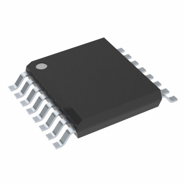
SN74ALS166DBR
ActivePARALLEL-LOAD 8-BIT SERIAL SHIFT REGISTERS
Deep-Dive with AI
Search across all available documentation for this part.

SN74ALS166DBR
ActivePARALLEL-LOAD 8-BIT SERIAL SHIFT REGISTERS
Deep-Dive with AI
Technical Specifications
Parameters and characteristics for this part
| Specification | SN74ALS166DBR |
|---|---|
| Function | Parallel or Serial to Serial |
| Logic Type | Shift Register |
| Mounting Type | Surface Mount |
| Number of Bits per Element | 8 |
| Number of Elements | 1 |
| Operating Temperature [Max] | 70 °C |
| Operating Temperature [Min] | 0 °C |
| Output Type | Push-Pull |
| Package / Case | 16-SSOP |
| Package / Case [custom] | 0.209 in |
| Package / Case [custom] | 5.3 mm |
| Supplier Device Package | 16-SSOP |
| Voltage - Supply [Max] | 5.5 V |
| Voltage - Supply [Min] | 4.5 V |
Pricing
Prices provided here are for design reference only. For realtime values and availability, please visit the distributors directly
| Distributor | Package | Quantity | $ | |
|---|---|---|---|---|
| Digikey | Cut Tape (CT) | 1 | $ 6.08 | |
| Digi-Reel® | 1 | $ 6.08 | ||
| Tape & Reel (TR) | 2000 | $ 3.05 | ||
| Texas Instruments | LARGE T&R | 1 | $ 4.81 | |
| 100 | $ 3.92 | |||
| 250 | $ 3.08 | |||
| 1000 | $ 2.61 | |||
Description
General part information
SN74ALS166 Series
The SN74ALS166 parallel-load 8-bit shift register is compatible with most other TTL logic families. All inputs are buffered to lower the drive requirements. Input clamping diodes minimize switching transients and simplify system design.
These parallel-in or serial-in, serial-out registers have a complexity of 77 equivalent gates on the chip. They feature gated clocks (CLK and CLK INH) inputs and an overriding clear (CLR\) input. The parallel-in or serial-in modes are established by the shift/load (SH/LD\) input. When high, SH/LD\ enables the serial data (SER) input and couples the eight flip-flops for serial shifting with each clock pulse. When low, the parallel (broadside) data (A-H) inputs are enabled and synchronous loading occurs on the next clock pulse. During parallel loading, serial data flow is inhibited. Clocking is accomplished on the low-to-high-level edge of the clock pulse through a two-input positive-NOR gate, permitting one input to be used as a clock-enable or clock-inhibit function. Holding either of the clock inputs high inhibits clocking; holding either low enables the other clock input. This allows the system clock to be free running and the register can be stopped on command with the clock input. CLK INH should be changed to the high level only when CLK is high. The buffered CLR\ overrides all other inputs, including CLK, and sets all flip-flops to zero.
The SN74ALS166 is characterized for operation from 0°C to 70°C.
Documents
Technical documentation and resources


