8T33FS6221EPGI
UnknownLOW VOLTAGE 1:20 DIFFERENTIAL PECL/HSTL CLOCK FANOUT BUFFER
Deep-Dive with AI
Search across all available documentation for this part.

8T33FS6221EPGI
UnknownLOW VOLTAGE 1:20 DIFFERENTIAL PECL/HSTL CLOCK FANOUT BUFFER
Deep-Dive with AI
Technical Specifications
Parameters and characteristics for this part
| Specification | 8T33FS6221EPGI |
|---|---|
| Differential - Input:Output [custom] | True |
| Differential - Input:Output [custom] | True |
| Frequency - Max [Max] | 2 GHz |
| Input | PECL, HSTL |
| Mounting Type | Surface Mount |
| Number of Circuits | 1 |
| Operating Temperature [Max] | 85 °C |
| Operating Temperature [Min] | -40 °C |
| Output | PECL |
| Package / Case | 52-LQFP Exposed Pad |
| Ratio - Input:Output [custom] | 1:20 |
| Supplier Device Package | 52-PTQFP (10x10) |
| Type | Fanout Buffer (Distribution) |
| Voltage - Supply [Max] | 2.625 V, 3.465 V |
| Voltage - Supply [Min] | 2.375 V, 3.135 V |
Pricing
Prices provided here are for design reference only. For realtime values and availability, please visit the distributors directly
| Distributor | Package | Quantity | $ | |
|---|---|---|---|---|
Description
General part information
8T33FS6221 Series
The 8T33FS6221 is a bipolar monolithic differential clock fanout buffer. Designed for most demanding clock distribution systems, the 8T33FS6221 supports various applications that require the distribution of precisely aligned differential clock signals. Using SiGe technology and a fully differential architecture, the device offers very low skew outputs and superior digital signal characteristics. Target applications for this clock driver are high-performance clock distribution in computing, networking, and telecommunication systems.
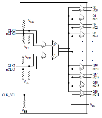
The 8T33FS6221 is designed for low-skew clock distribution systems and supports clock frequencies up to 2GHz. The device accepts two clock sources. The CLK0 input can be driven by PECL-compatible signals, the CLK1 input accepts HSTL-compatible signals. The selected input signal is distributed to 20 identical, differential PECL outputs. If VBBis connected to the nCLK0 or nCLK1 input and bypassed to GND by a 10nF capacitor, the 8T33FS6221 can be driven by single-ended PECL signals utilizing the VBBbias voltage output.
To meet the tight skew specification of the device, both outputs of a differential output pair should be terminated, even if only one output is used. In the case where not all ten outputs are used, the output pairs on the same package side as the parts being used on that side should be terminated.
Documents
Technical documentation and resources


