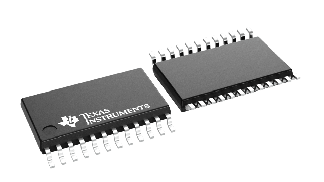
CLVCC4245AMPWREP
ActiveENHANCED PRODUCT OCTAL DUAL-SUPPLY BUS TRANSCEIVER W/CONFIGURABLE OUTPUT VOLTAGE AND 3S OUT
Deep-Dive with AI
Search across all available documentation for this part.

CLVCC4245AMPWREP
ActiveENHANCED PRODUCT OCTAL DUAL-SUPPLY BUS TRANSCEIVER W/CONFIGURABLE OUTPUT VOLTAGE AND 3S OUT
Technical Specifications
Parameters and characteristics for this part
| Specification | CLVCC4245AMPWREP |
|---|---|
| Channel Type | Bidirectional |
| Channels per Circuit | 8 |
| Mounting Type | Surface Mount |
| Number of Circuits | 1 |
| Operating Temperature [Max] | 125 °C |
| Operating Temperature [Min] | -55 °C |
| Output Type | Tri-State, Non-Inverted |
| Package / Case | 24-TSSOP |
| Package / Case | 0.173 in, 4.4 mm |
| Supplier Device Package | 24-TSSOP |
| Translator Type | Voltage Level |
| Voltage - VCCA [Max] | 5.5 V |
| Voltage - VCCA [Min] | 4.5 V |
| Voltage - VCCB [Max] | 5.5 V |
| Voltage - VCCB [Min] | 2.7 V |
Pricing
Prices provided here are for design reference only. For realtime values and availability, please visit the distributors directly
| Distributor | Package | Quantity | $ | |
|---|---|---|---|---|
| Digikey | Cut Tape (CT) | 1 | $ 3.72 | |
| 10 | $ 3.34 | |||
| 25 | $ 3.16 | |||
| 100 | $ 2.74 | |||
| 250 | $ 2.60 | |||
| 500 | $ 2.33 | |||
| 1000 | $ 1.97 | |||
| Digi-Reel® | 1 | $ 3.72 | ||
| 10 | $ 3.34 | |||
| 25 | $ 3.16 | |||
| 100 | $ 2.74 | |||
| 250 | $ 2.60 | |||
| 500 | $ 2.33 | |||
| 1000 | $ 1.97 | |||
| Tape & Reel (TR) | 2000 | $ 1.87 | ||
| Texas Instruments | LARGE T&R | 1 | $ 3.23 | |
| 100 | $ 2.83 | |||
| 250 | $ 1.98 | |||
| 1000 | $ 1.60 | |||
Description
General part information
SN74LVCC4245A-EP Series
The SN74LVCC4245A is an 8-bit (octal) noninverting bus transceiver that uses two separate power-supply rails. The A port (VCCA) is dedicated to accepting a 5-V supply level, and the configurable B port, which is designed to track VCCB, accepts voltages from 3 V to 5 V. This allows for translation from a 3.3-V to a 5-V environment and vice versa.The SN74LVCC4245A is designed for asynchronous communication between data buses. The device transmits data from the A bus to the B bus or from the B bus to the A bus, depending on the logic level at the direction-control (DIR) input. The output-enable (OE) input can be used to disable the device so the buses effectively are isolated. The control circuitry (DIR,OE) is powered by VCCA.
The SN74LVCC4245A is an 8-bit (octal) noninverting bus transceiver that uses two separate power-supply rails. The A port (VCCA) is dedicated to accepting a 5-V supply level, and the configurable B port, which is designed to track VCCB, accepts voltages from 3 V to 5 V. This allows for translation from a 3.3-V to a 5-V environment and vice versa.
The SN74LVCC4245A is designed for asynchronous communication between data buses. The device transmits data from the A bus to the B bus or from the B bus to the A bus, depending on the logic level at the direction-control (DIR) input. The output-enable (OE) input can be used to disable the device so the buses effectively are isolated. The control circuitry (DIR,OE) is powered by VCCA.
Documents
Technical documentation and resources


