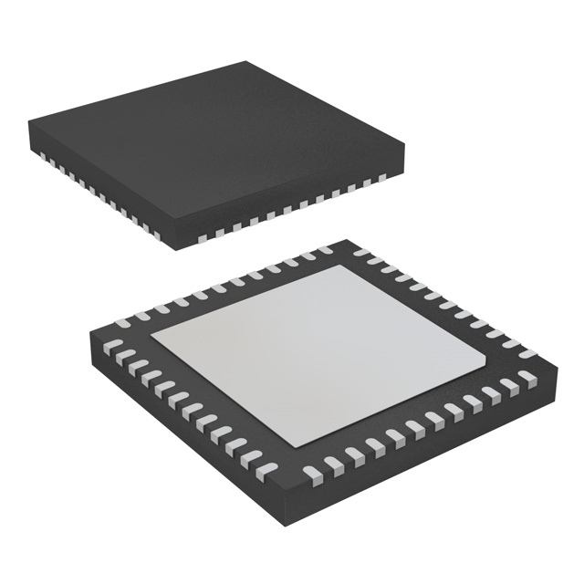
SN65MLVD040RGZT
Active4-CHANNEL HALF-DUPLEX M-LVDS LINE TRANSCEIVERS
Deep-Dive with AI
Search across all available documentation for this part.

SN65MLVD040RGZT
Active4-CHANNEL HALF-DUPLEX M-LVDS LINE TRANSCEIVERS
Technical Specifications
Parameters and characteristics for this part
| Specification | SN65MLVD040RGZT |
|---|---|
| Data Rate | 250 MBd |
| Duplex | Half |
| Mounting Type | Surface Mount |
| Number of Drivers/Receivers [custom] | 4 |
| Number of Drivers/Receivers [custom] | 4 |
| Operating Temperature [Max] | 85 °C |
| Operating Temperature [Min] | -40 °C |
| Package / Case | 48-VFQFN Exposed Pad |
| Protocol | Multipoint, LVDS |
| Receiver Hysteresis | 25 mV |
| Supplier Device Package | 48-VQFN (7x7) |
| Type | Transceiver |
| Voltage - Supply [Max] | 3.6 V |
| Voltage - Supply [Min] | 3 V |
Pricing
Prices provided here are for design reference only. For realtime values and availability, please visit the distributors directly
| Distributor | Package | Quantity | $ | |
|---|---|---|---|---|
| Digikey | Cut Tape (CT) | 1 | $ 10.80 | |
| 10 | $ 7.54 | |||
| 25 | $ 6.70 | |||
| 100 | $ 5.76 | |||
| Digi-Reel® | 1 | $ 10.80 | ||
| 10 | $ 7.54 | |||
| 25 | $ 6.70 | |||
| 100 | $ 5.76 | |||
| Tape & Reel (TR) | 250 | $ 5.31 | ||
| 500 | $ 5.03 | |||
| 750 | $ 4.89 | |||
| 1250 | $ 4.75 | |||
| Texas Instruments | SMALL T&R | 1 | $ 7.00 | |
| 100 | $ 5.70 | |||
| 250 | $ 4.48 | |||
| 1000 | $ 3.80 | |||
Description
General part information
SN65MLVD040 Series
The SN65MLVD040 provides four half-duplex transceivers for transmitting and receiving Multipoint-Low-Voltage Differential Signals in full compliance with the TIA/EIA-899 (M-LVDS) standard, which are optimized to operate at signaling rates up to 250Mbps. The driver outputs have been designed to support multipoint buses presenting loads as low as 30Ω and incorporates controlled transition times to allow for stubs off of the backplane transmission line.
The M-LVDS standard defines two types of receivers, designated as Type-1 and Type-2. Type-1 receivers have thresholds centered about zero with 25mV of hysteresis to prevent output oscillations with loss of input; Type-2 receivers implement a failsafe by using an offset threshold. The xFSEN pins is used to select the Type-1 and Type-2 receiver for each of the channels. In addition, the driver rise and fall times are between 1ns and 2ns, complying with the M-LVDS standard to provide operation at 250Mbps while also accommodating stubs on the bus. Receiver outputs are slew rate controlled to reduce EMI and crosstalk effects associated with large current surges. The M-LVDS standard allows for 32 nodes on the bus providing a high-speed replacement for RS-485 where lower common-mode can be tolerated or when higher signaling rates are needed.
The driver logic inputs and the receiver logic outputs are on separate pins rather than tied together as in some transceiver designs. The drivers have separate enables (DE) and so does the receivers ( RE). This arrangement of separate logic inputs, logic outputs, and enable pins allows for a listen-while-talking operation. The devices are characterized for operation from –40°C to 85°C.
Documents
Technical documentation and resources


