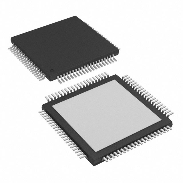
ADS5292IPFP
ActiveEIGHT-CHANNEL, 12-BIT, 80-MSPS ANALOG-TO-DIGITAL CONVERTER (ADC)
Deep-Dive with AI
Search across all available documentation for this part.

ADS5292IPFP
ActiveEIGHT-CHANNEL, 12-BIT, 80-MSPS ANALOG-TO-DIGITAL CONVERTER (ADC)
Deep-Dive with AI
Technical Specifications
Parameters and characteristics for this part
| Specification | ADS5292IPFP |
|---|---|
| Architecture | Pipelined |
| Configuration | S/H-ADC |
| Data Interface | LVDS - Serial |
| Features | Simultaneous Sampling |
| Input Type | Differential |
| Mounting Type | Surface Mount |
| Number of A/D Converters | 8 |
| Number of Bits | 12 bits |
| Number of Inputs | 8 |
| Operating Temperature [Max] | 85 °C |
| Operating Temperature [Min] | -40 °C |
| Package / Case | 80-TQFP Exposed Pad |
| Ratio - S/H:ADC | 1:1 |
| Reference Type | External, Internal |
| Sampling Rate (Per Second) | 80 M |
| Supplier Device Package | 80-HTQFP (12x12) |
| Voltage - Supply, Analog [Max] | 1.9 V |
| Voltage - Supply, Analog [Min] | 1.7 V |
| Voltage - Supply, Digital [Max] | 1.9 V |
| Voltage - Supply, Digital [Min] | 1.7 V |
Pricing
Prices provided here are for design reference only. For realtime values and availability, please visit the distributors directly
| Distributor | Package | Quantity | $ | |
|---|---|---|---|---|
| Digikey | Tube | 96 | $ 84.22 | |
| Texas Instruments | JEDEC TRAY (5+1) | 1 | $ 83.39 | |
| 100 | $ 80.88 | |||
| 250 | $ 67.34 | |||
| 1000 | $ 62.70 | |||
Description
General part information
ADS5292 Series
Using CMOS process technology and innovative circuit techniques, the ADS5292 is a low power 80MSPS 8-Channel ADC. Low power consumption, high SNR, low SFDR, and consistent overload recovery allow users to design high performance systems.
The ADS5292 has a digital processing block that integrates several commonly used digital functions for improving system performance. It includes a digital filter module that has built-in decimation filters (with low-pass, high-pass and band-pass characteristics). The decimation rate is also programmable (by 2, by 4, or by 8). This makes it useful for narrow-band applications, where the filters can be used conveniently to improve SNR and knock-off harmonics, while at the same time reducing the output data rate. The device includes an averaging mode where two channels (or even four channels) can be averaged to improve SNR.
Serial LVDS outputs reduce the number of interface lines and enable the highest system integration. The digital data from each channel ADC can be output over one or two wires of LVDS output lines depending on the ADC sampling rate. This 2-wire interface helps keep the serial data rate low, allowing low cost FPGA based receivers to be used even at high sample rate. A unique feature is the programmable mapping module that allows flexible mapping between the input channels and the LVDS output pins. This helps greatly reduce the complexity of LVDS output routing and can potentially result in cheaper system boards by reducing the number of PCB layers.
Documents
Technical documentation and resources


