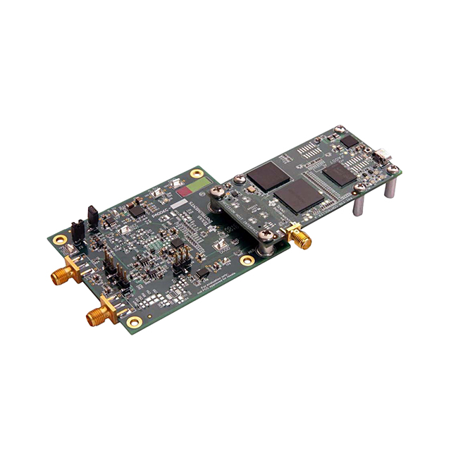
ADS8910BEVM-PDK
ObsoleteANALOG TO DIGITAL CONVERTER EVAL
Deep-Dive with AI
Search across all available documentation for this part.

ADS8910BEVM-PDK
ObsoleteANALOG TO DIGITAL CONVERTER EVAL
Deep-Dive with AI
Technical Specifications
Parameters and characteristics for this part
| Specification | ADS8910BEVM-PDK |
|---|---|
| Data Interface | SPI |
| Input Range | ±VREF |
| Number of A/D Converters | 1 |
| Power (Typ) @ Conditions | 21 mW |
| Sampling Rate (Per Second) | 1 M |
| Supplied Contents | Cable(s), Board(s) |
| Utilized IC / Part | ADS8910B |
Pricing
Prices provided here are for design reference only. For realtime values and availability, please visit the distributors directly
| Distributor | Package | Quantity | $ | |
|---|---|---|---|---|
Description
General part information
ADS8910B Series
The ADS8910B, ADS8912B, and ADS8914B (ADS891xB) belong to a family of pin-to-pin compatible, high-speed, single-channel, high-precision, 18-bit successive approximation register (SAR) analog-to-digital convertors (ADCs) with an integrated reference buffer and integrated low-dropout regulator (LDO). The device family includes the ADS890xB (20-bit) and ADS892xB (16-bit) resolution variants.
The ADS891xB boost analog performance while maintaining high-resolution data transfer by using TI’s enhanced-SPI feature. Enhanced-SPI enables the ADS89xxB to achieve high throughput at lower clock speeds, thereby simplifying the board layout and lowering system cost. Enhanced-SPI also simplifies clocking-in of data, thereby making this device an excellent choice for applications involving FPGAs, DSPs. The ADS89xxB is compatible with a standard SPI Interface.
The ADS891xB has an internal data parity feature that can be appended to the ADC data output. ADC data validation by the host, using parity bits, improves system reliability.
Documents
Technical documentation and resources
No documents available


