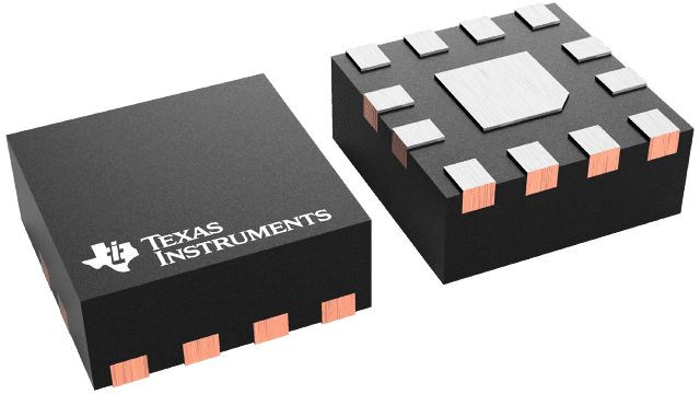
LMH9226IRRLR
ActiveSINGLE-ENDED TO DIFFERENTIAL 2.3 - 2.9 GHZ LOW-POWER ADC DRIVER WITH INTEGRATED BALUN
Deep-Dive with AI
Search across all available documentation for this part.

LMH9226IRRLR
ActiveSINGLE-ENDED TO DIFFERENTIAL 2.3 - 2.9 GHZ LOW-POWER ADC DRIVER WITH INTEGRATED BALUN
Technical Specifications
Parameters and characteristics for this part
| Specification | LMH9226IRRLR |
|---|---|
| Current - Supply | 84 mA |
| Frequency [Max] | 2.9 GHz |
| Frequency [Min] | 2.3 GHz |
| Gain | 17 dBi |
| Mounting Type | Surface Mount |
| Noise Figure | 3 dB |
| P1dB | 17.5 dBm |
| Package / Case | 12-WFQFN Exposed Pad |
| RF Type | General Purpose |
| Supplier Device Package | 12-WQFN (2x2) |
| Test Frequency | 2.6 GHz |
| Voltage - Supply [Max] | 3.45 V |
| Voltage - Supply [Min] | 3.15 V |
Pricing
Prices provided here are for design reference only. For realtime values and availability, please visit the distributors directly
| Distributor | Package | Quantity | $ | |
|---|---|---|---|---|
| Digikey | Cut Tape (CT) | 1 | $ 2.80 | |
| 10 | $ 2.52 | |||
| 25 | $ 2.38 | |||
| 100 | $ 2.06 | |||
| 250 | $ 1.96 | |||
| 500 | $ 1.76 | |||
| 1000 | $ 1.48 | |||
| Digi-Reel® | 1 | $ 2.80 | ||
| 10 | $ 2.52 | |||
| 25 | $ 2.38 | |||
| 100 | $ 2.06 | |||
| 250 | $ 1.96 | |||
| 500 | $ 1.76 | |||
| 1000 | $ 1.48 | |||
| Tape & Reel (TR) | 3000 | $ 1.31 | ||
| Texas Instruments | LARGE T&R | 1 | $ 2.12 | |
| 100 | $ 1.85 | |||
| 250 | $ 1.30 | |||
| 1000 | $ 1.05 | |||
Description
General part information
LMH9226 Series
The LMH9226 is high-performance, single-channel, single-ended, 50-Ω input to differential 50-Ω or 100-Ω output RF gain block amplifier supporting a 2.3-GHz to 2.9-GHz frequency band. The device is well suited to meet requirements for 5G m-MIMO or small cell base station applications. The device integrates the functionality of a single-ended input and output RF gain block followed by a passive balun, where the device is mainly used in the final stage of a receiver signal chain to drive the full-scale voltage of an analog-to-differential converter (ADC) differential input.
The LMH9226 provides 17-dB typical gain with excellent linearity performance of 35-dBm output IP3 at 2.6 GHz, and maintains less than a 3-dB noise figure across the entire 1-dB bandwidth of 400 MHz. The device is internally matched for a 50-Ω impedance at the single-ended input. The differential output can easily interface to a 50-Ω impedance without any external matching circuitry. For 100-Ω impedance matching, an external matching circuitry is required that typically results in a 0.3-dB gain loss at 2.6 GHz.
Operating on a single 3.3-V supply, the device consumes approximately 275 mW of stand-by power, making the device suitable for high-density, 5G, massive multiple-input and multiple-output (MIMO) applications. Also, the device is available in a space-saving, 2-mm × 2-mm, 12-pin WQFN package. The device is rated for an operating temperature of up to 105°C to provide a robust system design. A 1.8-V JEDEC compliant power-down pin is available for fast power-down and power-up of the device that is suitable for time division duplex (TDD) systems.


