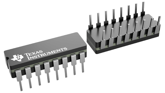
CD4015BF3A
ActiveSHIFT REGISTER DUAL 4-BIT SERIAL TO PARALLEL 16-PIN CDIP TUBE
Deep-Dive with AI
Search across all available documentation for this part.

CD4015BF3A
ActiveSHIFT REGISTER DUAL 4-BIT SERIAL TO PARALLEL 16-PIN CDIP TUBE
Deep-Dive with AI
Technical Specifications
Parameters and characteristics for this part
| Specification | CD4015BF3A |
|---|---|
| Function | Serial to Parallel |
| Logic Type | Shift Register |
| Mounting Type | Through Hole |
| Number of Bits per Element | 4 |
| Number of Elements | 2 |
| Operating Temperature [Max] | 125 °C |
| Operating Temperature [Min] | -55 °C |
| Output Type | Non-Inverted |
| Package / Case | 7.62 mm, 0.3 in |
| Package / Case | 16-CDIP |
| Supplier Device Package | 16-CDIP |
| Voltage - Supply [Max] | 18 V |
| Voltage - Supply [Min] | 3 V |
Pricing
Prices provided here are for design reference only. For realtime values and availability, please visit the distributors directly
| Distributor | Package | Quantity | $ | |
|---|---|---|---|---|
| Arrow | N/A | 25 | $ 11.17 | |
| Texas Instruments | TUBE | 1 | $ 15.89 | |
| 100 | $ 13.88 | |||
| 250 | $ 10.70 | |||
| 1000 | $ 9.57 | |||
Description
General part information
CD4015B-MIL Series
CD4015B consists of two identical, independent, 4-stage serial-input/parallel-output registers. Each register has independent CLOCK and RESET inputs as well as a single serial DATA input. "Q" outputs are available from each of the four stages on both registers. All register stages are D-type, master-slave flip-flops. The logic level present at the DATA input is transferred into the first register stage and shifted over one stage at each positive-going clock transition. Resetting of all stages is accomplished by a high level on the reset line. Register expansion to 8 stages using one CD4015B package, or to more than 8 stages using additional CD4015B’s is possible.
The CD4015B-series types are supplied in 16-lead hermetic dual-in-line ceramic packages (F3A suffix), 16-lead dual-in-line plastic package (E suffix), 16-lead small-outline packages (M, M96, MT, and NSR suffixes), and 16-lead thin shrink small-outline packages (PW and PWR suffixes).
CD4015B consists of two identical, independent, 4-stage serial-input/parallel-output registers. Each register has independent CLOCK and RESET inputs as well as a single serial DATA input. "Q" outputs are available from each of the four stages on both registers. All register stages are D-type, master-slave flip-flops. The logic level present at the DATA input is transferred into the first register stage and shifted over one stage at each positive-going clock transition. Resetting of all stages is accomplished by a high level on the reset line. Register expansion to 8 stages using one CD4015B package, or to more than 8 stages using additional CD4015B’s is possible.
Documents
Technical documentation and resources


