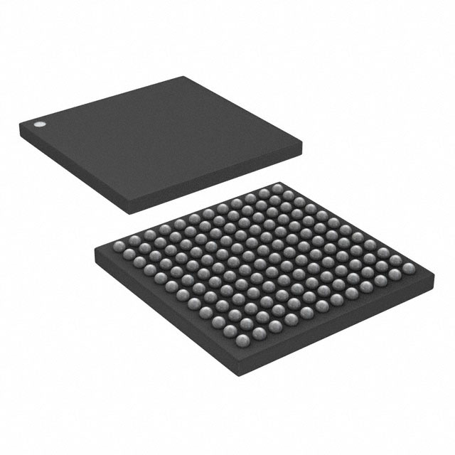
MAX5857EXE+
Obsolete16-BIT, 5.9GSPS WIDEBAND INTERPOLATING AND MODULATING RF DAC WITH JESD204B INTERFACE
Deep-Dive with AI
Search across all available documentation for this part.

MAX5857EXE+
Obsolete16-BIT, 5.9GSPS WIDEBAND INTERPOLATING AND MODULATING RF DAC WITH JESD204B INTERFACE
Deep-Dive with AI
Technical Specifications
Parameters and characteristics for this part
| Specification | MAX5857EXE+ |
|---|---|
| Frequency [Max] | 2.6 GHz |
| Frequency [Min] | 0 Hz |
| Function | VCO/PLL Synthesizer |
| Mounting Type | Surface Mount |
| Package / Case | FCCSPBGA, 144-LFBGA |
| RF Type | General Purpose |
| Supplier Device Package | 144-FCCSP (10x10) |
Pricing
Prices provided here are for design reference only. For realtime values and availability, please visit the distributors directly
| Distributor | Package | Quantity | $ | |
|---|---|---|---|---|
| Digikey | N/A | 0 | $ 160.91 | |
Description
General part information
MAX5857 Series
The MAX5857 high-performance, interpolating and modulating, 16-bit, 5.9Gsps RF DAC can directly synthesize up to 1.2GHz of instantaneous bandwidth from DC to frequencies greater than 2.6GHz. The device is optimized for cable access and digital video broadcast applications and meets spectral emission requirements for a broad set of radio transmitters and modulators including DOCSIS 3.1/3.0, DVB-C2, DVB-T2, DVB-S2X, ISDB-T, and EPoC.The device integrates interpolation filters, a digital quadrature modulator, a numerically controlled oscillator (NCO), clock multiplying PLL+VCO and a 14-bit RF DAC core. The 4x linear phase interpolation filter simplifies reconstruction filtering, while enhancing passband dynamic performance and reducing the input data bandwidth required from an FPGA. The NCO allows for fully agile modulation of the input baseband signal for direct RF synthesis. The complex data path can be bypassed to access the RF DAC core directly.The MAX5857 input interface accepts 16-bit input data through a six-lane JESD204B SerDes data input interface that is Subclass-0. The interface can be configured for 3, 4, 5, or 6 lanes and supports data rates up to 9.8304Gbps to optimize the I/O lane count and speed.The MAX5857 clock input has a flexible interface that accepts a differential sine-wave or square-wave input clock signal up to 5.9GHz. A bypassable clock multiplying PLL and VCO can be used to internally generate the high-frequency sampling clock using a reference frequency between 245.76MHz and 1.475GHz. The device provides a divided reference clock to ensure synchronization between the data source and the DAC.The integrated RF DAC uses a differential current-steering architecture that includes a differential 50Ω internal termination and can produce a 3.2dBm full-scale output signal level on a 50Ω external load. Operating from 1.0V and 1.8V power supplies, the device consumes 2.7W at 4.9Gsps. The device is offered in a compact 144-pin, 10mm x 10mm, FCCSP package and is specified for the extended industrial temperature range (-40°C to +85°C).ApplicationsDigital Video Broadcast ModulatorsDOCSIS 3.1 Remote PHY and CCAPDVB-C2/DVB-T2/DVB-S2X/ISDB-TEthernet PON over Coax (EPoC)InstrumentationPoint-to-Point Wireless


