Deep-Dive with AI
Search across all available documentation for this part.

Deep-Dive with AI
Technical Specifications
Parameters and characteristics for this part
| Specification | MC14049UBDR2G |
|---|---|
| Current - Output High, Low [custom] | 10 mA |
| Current - Output High, Low [custom] | 40 mA |
| Current - Quiescent (Max) [Max] | 4 µA |
| Input Logic Level - High [Max] | 12.5 V |
| Input Logic Level - High [Min] | 4 V |
| Input Logic Level - Low [Max] | 2.5 V |
| Input Logic Level - Low [Min] | 1 V |
| Logic Type | Inverter |
| Mounting Type | Surface Mount |
| Number of Circuits | 6 |
| Number of Inputs | 1 |
| Operating Temperature [Max] | 125 °C |
| Operating Temperature [Min] | -55 °C |
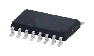
| Package / Case | 16-SOIC |
| Package / Case [x] | 0.154 in |
| Package / Case [y] | 3.9 mm |
| Supplier Device Package | 16-SOIC |
| Voltage - Supply [Max] | 18 V |
| Voltage - Supply [Min] | 3 V |
Pricing
Prices provided here are for design reference only. For realtime values and availability, please visit the distributors directly
| Distributor | Package | Quantity | $ | |
|---|---|---|---|---|
| Digikey | Cut Tape (CT) | 1 | $ 1.03 | |
| 10 | $ 0.61 | |||
| 25 | $ 0.51 | |||
| 100 | $ 0.39 | |||
| 250 | $ 0.34 | |||
| 500 | $ 0.30 | |||
| 1000 | $ 0.28 | |||
| Digi-Reel® | 1 | $ 1.03 | ||
| 10 | $ 0.61 | |||
| 25 | $ 0.51 | |||
| 100 | $ 0.39 | |||
| 250 | $ 0.34 | |||
| 500 | $ 0.30 | |||
| 1000 | $ 0.28 | |||
| Tape & Reel (TR) | 2500 | $ 0.25 | ||
| 5000 | $ 0.23 | |||
| 7500 | $ 0.22 | |||
| 12500 | $ 0.21 | |||
| 17500 | $ 0.21 | |||
| 25000 | $ 0.20 | |||
| Newark | Each (Supplied on Cut Tape) | 1 | $ 0.35 | |
| 10 | $ 0.35 | |||
| 25 | $ 0.33 | |||
| 50 | $ 0.31 | |||
| 100 | $ 0.29 | |||
| ON Semiconductor | N/A | 1 | $ 0.21 | |
Description
General part information
MC14049UB Series
The MC14049B Hex Inverter/Buffer and MC14050B Noninverting Hex Buffer are constructed with MOS P-Channel and N-Channel enhancement mode devices in a single monolithic structure. These complementary MOS devices find primary use where low power dissipation and/or high noise immunity is desired. These devices provide logic level conversion using only one supply voltage, VDD.The input-signal high level (VIH) can exceed the VDDsupply voltage for logic level conversions. Two TTL/DTL loads can be driven when the devices are used as a CMOS-to-TTL/DTL converter (VDD= 5.0 V, VOL<= 0.4 V, IOL>= 3.2 mA).Note that pins 13 and 16 are not connected internally on these devices; consequently connections to these terminals will not affect circuit operation.
Documents
Technical documentation and resources


