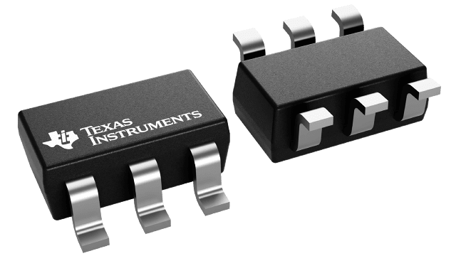
SN74LXC1T45DBVR
ActiveSINGLE-BIT DUAL-SUPPLY BUS TRANSCEIVER WITH CONFIGURABLE VOLTAGE-LEVEL SHIFTING AND 3-STATE OUTPUTS
Deep-Dive with AI
Search across all available documentation for this part.

SN74LXC1T45DBVR
ActiveSINGLE-BIT DUAL-SUPPLY BUS TRANSCEIVER WITH CONFIGURABLE VOLTAGE-LEVEL SHIFTING AND 3-STATE OUTPUTS
Technical Specifications
Parameters and characteristics for this part
| Specification | SN74LXC1T45DBVR |
|---|---|
| Channel Type | Bidirectional |
| Channels per Circuit | 1 |
| Mounting Type | Surface Mount |
| Number of Circuits | 1 |
| Operating Temperature [Max] | 125 °C |
| Operating Temperature [Min] | -40 °C |
| Output Type | Non-Inverted |
| Package / Case | SOT-23-6 |
| Supplier Device Package | SOT-23-6 |
| Translator Type | Voltage Level |
| Voltage - VCCA [Max] | 5.5 V |
| Voltage - VCCA [Min] | 1.1 V |
Pricing
Prices provided here are for design reference only. For realtime values and availability, please visit the distributors directly
| Distributor | Package | Quantity | $ | |
|---|---|---|---|---|
| Digikey | Cut Tape (CT) | 1 | $ 0.62 | |
| 10 | $ 0.54 | |||
| 25 | $ 0.50 | |||
| 100 | $ 0.40 | |||
| 250 | $ 0.37 | |||
| 500 | $ 0.31 | |||
| 1000 | $ 0.24 | |||
| Digi-Reel® | 1 | $ 0.62 | ||
| 10 | $ 0.54 | |||
| 25 | $ 0.50 | |||
| 100 | $ 0.40 | |||
| 250 | $ 0.37 | |||
| 500 | $ 0.31 | |||
| 1000 | $ 0.24 | |||
| Tape & Reel (TR) | 3000 | $ 0.22 | ||
| 6000 | $ 0.21 | |||
| 15000 | $ 0.19 | |||
| 30000 | $ 0.18 | |||
| Texas Instruments | LARGE T&R | 1 | $ 0.35 | |
| 100 | $ 0.24 | |||
| 250 | $ 0.18 | |||
| 1000 | $ 0.12 | |||
Description
General part information
SN74LXC1T45 Series
The SN74LXC1T45 is a 1-bit, dual-supply noninverting bidirectional voltage level translation device. The I/O pin A and control pin (DIR) are referenced to VCCAlogic levels, and the I/O pin B are referenced to VCCBlogic levels. The A pin is able to accept I/O voltages ranging from 1.1 V to 5.5 V, while the B pin can accept I/O voltages from 1.1 V to 5.5 V. A high on DIR allows data transmission from A to B and a low on DIR allows data transmission from B to A. SeeDevice Functional Modesfor a summary of the operation of the control logic.
The SN74LXC1T45 is a 1-bit, dual-supply noninverting bidirectional voltage level translation device. The I/O pin A and control pin (DIR) are referenced to VCCAlogic levels, and the I/O pin B are referenced to VCCBlogic levels. The A pin is able to accept I/O voltages ranging from 1.1 V to 5.5 V, while the B pin can accept I/O voltages from 1.1 V to 5.5 V. A high on DIR allows data transmission from A to B and a low on DIR allows data transmission from B to A. SeeDevice Functional Modesfor a summary of the operation of the control logic.
Documents
Technical documentation and resources


