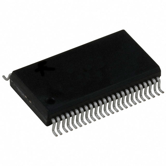
SN74AUC16373DGGR
ActiveIC: DIGITAL; D LATCH; CH: 16; CMOS; 0.8÷2.7VDC; SMD; TSSOP48; AUC
Deep-Dive with AI
Search across all available documentation for this part.

SN74AUC16373DGGR
ActiveIC: DIGITAL; D LATCH; CH: 16; CMOS; 0.8÷2.7VDC; SMD; TSSOP48; AUC
Deep-Dive with AI
Technical Specifications
Parameters and characteristics for this part
| Specification | SN74AUC16373DGGR |
|---|---|
| Circuit [custom] | 8 |
| Circuit [custom] | 8 |
| Current - Output High, Low [custom] | 9 mA |
| Current - Output High, Low [custom] | 9 mA |
| Delay Time - Propagation | 8 ns |
| Independent Circuits | 2 |
| Logic Type | D-Type Transparent Latch |
| Mounting Type | Surface Mount |
| Operating Temperature [Max] | 85 °C |
| Operating Temperature [Min] | -40 °C |
| Output Type | Tri-State |
| Package / Case | 48-TFSOP |
| Package / Case | 0.24 in |
| Package / Case [custom] | 6.1 mm |
| Supplier Device Package | 48-TSSOP |
| Voltage - Supply [Max] | 2.7 V |
| Voltage - Supply [Min] | 0.8 V |
Pricing
Prices provided here are for design reference only. For realtime values and availability, please visit the distributors directly
| Distributor | Package | Quantity | $ | |
|---|---|---|---|---|
| Digikey | Cut Tape (CT) | 1 | $ 2.75 | |
| 10 | $ 2.47 | |||
| 25 | $ 2.33 | |||
| 100 | $ 1.99 | |||
| 250 | $ 1.87 | |||
| 500 | $ 1.63 | |||
| 1000 | $ 1.35 | |||
| Digi-Reel® | 1 | $ 2.75 | ||
| 10 | $ 2.47 | |||
| 25 | $ 2.33 | |||
| 100 | $ 1.99 | |||
| 250 | $ 1.87 | |||
| 500 | $ 1.63 | |||
| 1000 | $ 1.35 | |||
| Tape & Reel (TR) | 2000 | $ 1.27 | ||
| 4000 | $ 1.20 | |||
| 6000 | $ 1.17 | |||
| TME | N/A | 1 | $ 15.33 | |
| 3 | $ 14.19 | |||
| 5 | $ 13.06 | |||
| Texas Instruments | LARGE T&R | 1 | $ 2.07 | |
| 100 | $ 1.71 | |||
| 250 | $ 1.23 | |||
| 1000 | $ 0.92 | |||
Description
General part information
SN74AUC16373 Series
This 16-bit transparent D-type latch is operational at 0.8-V to 2.7-V VCC, but is designed specifically for 1.65-V to 1.95-V VCCoperation.
The SN74AUC16373 is particularly suitable for implementing buffer registers, I/O ports, bidirectional bus drivers, and working registers. The device can be used as two 8-bit latches or one 16-bit latch. When the latch-enable (LE) input is high, the Q outputs follow the data (D) inputs. When LE is taken low, the Q outputs are latched at the levels set up at the D inputs.
A buffered output-enable (OE)\ input can be used to place the eight outputs in either a normal logic state (high or low logic levels) or the high-impedance state. In the high-impedance state, the outputs neither load nor drive the bus lines significantly. The high-impedance state and increased drive provide the capability to drive bus lines without interface or pullup components.
Documents
Technical documentation and resources


