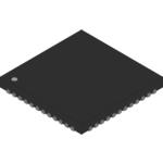
MAX5865ETM+
ActiveULTRA-LOW-POWER, HIGH-DYNAMIC-PERFORMANCE, 40MSPS ANALOG FRONT END
Deep-Dive with AI
Search across all available documentation for this part.

MAX5865ETM+
ActiveULTRA-LOW-POWER, HIGH-DYNAMIC-PERFORMANCE, 40MSPS ANALOG FRONT END
Technical Specifications
Parameters and characteristics for this part
| Specification | MAX5865ETM+ |
|---|---|
| Mounting Type | Surface Mount |
| Number of Bits | 10 |
| Number of Channels [custom] | 4 |
| Package / Case | 48-WFQFN Exposed Pad |
| Power (Watts) | 2.1 W |
| Supplier Device Package | 48-TQFN (7x7) |
| Voltage - Supply, Analog [Max] | 3.3 V |
| Voltage - Supply, Analog [Min] | 2.7 V |
| Voltage - Supply, Digital [Max] [custom] | 3.3 V |
| Voltage - Supply, Digital [Min] [custom] | 2.7 V |
Pricing
Prices provided here are for design reference only. For realtime values and availability, please visit the distributors directly
| Distributor | Package | Quantity | $ | |
|---|---|---|---|---|
| Digikey | N/A | 172 | $ 18.97 | |
| 279 | $ 18.97 | |||
| Tube | 1 | $ 18.20 | ||
| 10 | $ 13.15 | |||
| 25 | $ 11.85 | |||
| 100 | $ 10.40 | |||
| 250 | $ 9.70 | |||
| 500 | $ 9.29 | |||
Description
General part information
MAX5865 Series
The MAX5865 ultra-low-power, highly integrated analog front end is ideal for portable communication equipment such as handsets, PDAs, WLAN, and 3G wireless terminals. The MAX5865 integrates dual 8-bit receive ADCs and dual 10-bit transmit DACs while providing the highest dynamic performance at ultra-low power. The ADCs' analog I-Q input amplifiers are fully differential and accept 1VP-Pfull-scale signals. Typical I-Q channel phase matching is ±0.2° and amplitude matching is ±0.05dB. The ADCs feature 48.4dB SINAD and 70dBc spurious-free dynamic range (SFDR) at fIN= 5.5MHz and fCLK= 40MHz. The DACs' analog I-Q outputs are fully differential with ±400mV full-scale output, and 1.4V common-mode level. Typical I-Q channel phase matching is ±0.15° and gain matching is ±0.05dB. The DACs also feature dual 10-bit resolution with 72dBc SFDR, and 57dB SNR at fOUT= 2.2MHz and fCLK= 40MHz.The ADCs and DACs operate simultaneously or independently for frequency-division duplex (FDD) and time-division duplex (TDD) modes. A 3-wire serial interface controls power-down and transceiver modes of operation. The typical operating power is 75.6mW at fCLK= 40Msps with the ADCs and DACs operating simultaneously in transceiver mode. The MAX5865 features an internal 1.024V voltage reference that is stable over the entire operating power-supply range and temperature range. The MAX5865 operates on a +2.7V to +3.3V analog power supply and a +1.8V to +3.3V digital I/O power supply for logic compatibility. The quiescent current is 8.5mA in idle mode and 1µA in shutdown mode. The MAX5865 is specified for the extended (-40°C to +85°C) temperature range and is available in a 48-pin thin QFN package.Applications3G Wireless TerminalsFixed/Mobile Broadband Wireless ModemsNarrowband/Wideband CDMA HandsetsPDAs
Documents
Technical documentation and resources


