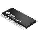
SN74AVC16835DGGR
ObsoleteBUS XCVR SINGLE 18-CH 3-ST 56-PIN TSSOP T/R
Deep-Dive with AI
Search across all available documentation for this part.

SN74AVC16835DGGR
ObsoleteBUS XCVR SINGLE 18-CH 3-ST 56-PIN TSSOP T/R
Deep-Dive with AI
Technical Specifications
Parameters and characteristics for this part
| Specification | SN74AVC16835DGGR |
|---|---|
| Current - Output High, Low [custom] | 12 mA |
| Current - Output High, Low [custom] | 12 mA |
| Logic Type | Universal Bus Driver |
| Mounting Type | Surface Mount |
| Number of Circuits | 18 Bit |
| Operating Temperature [Max] | 85 °C |
| Operating Temperature [Min] | -40 °C |
| Package / Case | 6.1 mm |
| Package / Case | 0.24 in |
| Package / Case | 56-TFSOP |
| Supplier Device Package | 56-TSSOP |
| Voltage - Supply [Max] | 3.6 V |
| Voltage - Supply [Min] | 1.4 V |
Pricing
Prices provided here are for design reference only. For realtime values and availability, please visit the distributors directly
| Distributor | Package | Quantity | $ | |
|---|---|---|---|---|
Description
General part information
SN74AVC16835 Series
A Dynamic Output Control (DOC™) circuit is implemented, which, during the transition, initially lowers the output impedance to effectively drive the load and, subsequently, raises the impedance to reduce noise. Figure 1 shows typical VOLvs IOLand VOHvs IOHcurves to illustrate the output impedance and drive capability of the circuit. At the beginning of the signal transition, the DOC circuit provides a maximum dynamic drive that is equivalent to a high-drive standard-output device. For more information, refer to the TI application reports,AVC Logic Family Technology and Applications, literature number SCEA006, andDynamic Output Control (DOC™) Circuitry Technology and Applications, literature number SCEA009.
This 18-bit universal bus driver is operational at 1.2-V to 3.6-V VCC, but is designed specifically for 1.65-V to 3.6-V VCCoperation.
Data flow from A to Y is controlled by the output-enable (OE)\ input. The device operates in the transparent mode when the latch-enable (LE) input is high. The A data is latched if the clock (CLK) input is held at a high or low logic level. If LE is low, the A data is stored in the latch/flip-flop on the low-to-high transition of CLK. When OE\ is high, the outputs are in the high-impedance state.
Documents
Technical documentation and resources


