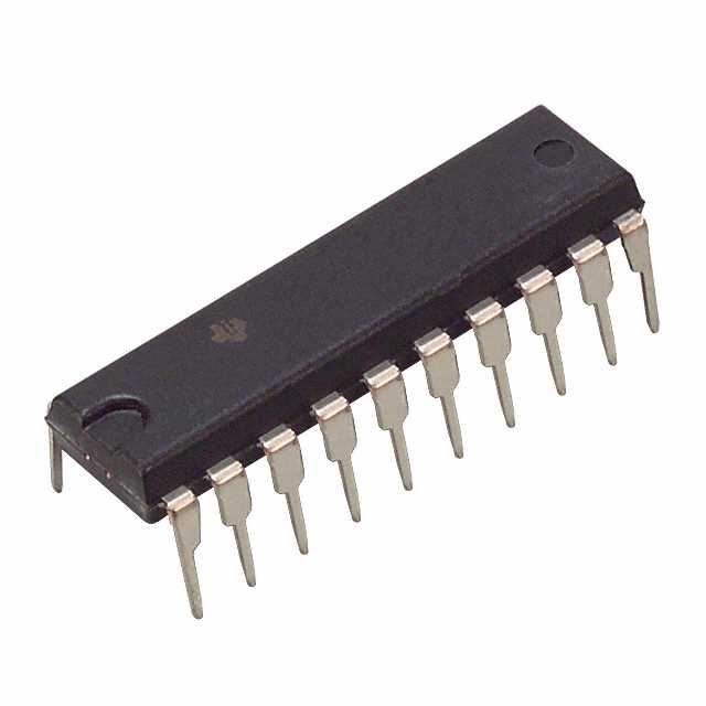
CY74FCT541ATPC
Active8-CH, 4.75-V TO 5.25-V BUFFERS WITH TTL-COMPATIBLE CMOS INPUTS AND 3-STATE OUTPUTS
Deep-Dive with AI
Search across all available documentation for this part.

CY74FCT541ATPC
Active8-CH, 4.75-V TO 5.25-V BUFFERS WITH TTL-COMPATIBLE CMOS INPUTS AND 3-STATE OUTPUTS
Technical Specifications
Parameters and characteristics for this part
| Specification | CY74FCT541ATPC |
|---|---|
| Current - Output High, Low [custom] | 64 mA |
| Current - Output High, Low [custom] | 32 mA |
| Logic Type | Buffer, Non-Inverting |
| Mounting Type | Through Hole |
| Number of Bits per Element | 8 |
| Number of Elements | 1 |
| Operating Temperature [Max] | 85 °C |
| Operating Temperature [Min] | -40 °C |
| Output Type | 3-State |
| Package / Case | 20-DIP |
| Package / Case | 7.62 mm |
| Package / Case | 0.3 in |
| Supplier Device Package | 20-PDIP |
| Voltage - Supply [Max] | 5.25 V |
| Voltage - Supply [Min] | 4.75 V |
Pricing
Prices provided here are for design reference only. For realtime values and availability, please visit the distributors directly
| Distributor | Package | Quantity | $ | |
|---|---|---|---|---|
| Digikey | Tube | 1 | $ 0.74 | |
| 20 | $ 0.66 | |||
| 40 | $ 0.63 | |||
| 100 | $ 0.51 | |||
| 260 | $ 0.48 | |||
| 500 | $ 0.42 | |||
| 1000 | $ 0.39 | |||
| Texas Instruments | TUBE | 1 | $ 0.95 | |
| 100 | $ 0.73 | |||
| 250 | $ 0.54 | |||
| 1000 | $ 0.38 | |||
Description
General part information
CY74FCT541T Series
The CD74FCT541 is an octal buffer/driver with 3-state outputs that is ideal for driving bus lines or buffer memory address registers and uses a small-geometry BiCMOS technology. The output stage is a combination of bipolar and CMOS transistors that limits the output high level to two diode drops below VCC. This resultant lowering of output swing (0 V to 3.7 V) reduces power-bus ringing [a source of electromagnetic interference (EMI)] and minimizes VCCbounce and ground bounce and their effects during simultaneous output switching. The output configuration also enhances switching speed and is capable of sinking 64 mA.
The 3-state control gate is a two-input AND gate with active-low inputs, so that if either output-enable (OE1\ or OE2\) input is high, all corresponding outputs are in the high-impedance state. The outputs provide noninverted data when they are not in the high-impedance state.
To ensure the high-impedance state during power up or power down, OE\ should be tied to VCCthrough a pullup resistor; the minimum value of the resistor is determined by the current-sinking capability of the driver.
Documents
Technical documentation and resources


