Deep-Dive with AI
Search across all available documentation for this part.

Deep-Dive with AI
Technical Specifications
Parameters and characteristics for this part
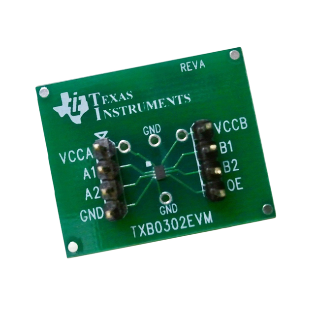
| Specification | TXB0302EVM |
|---|---|
| Contents | Board(s) |
| Embedded | False |
| Function | Logic-Level Translator |
| Primary Attributes | Bi-Directional, 2 Bit |
| Supplied Contents | Board(s) |
| Type | Interface |
| Utilized IC / Part | TXB0302 |
Pricing
Prices provided here are for design reference only. For realtime values and availability, please visit the distributors directly
| Distributor | Package | Quantity | $ | |
|---|---|---|---|---|
| Digikey | Box | 1 | $ 24.00 | |
| N/A | 2 | $ 24.00 | ||
Description
General part information
TXB0302 Series
This 2-bit noninverting translator uses two separate configurable power-supply rails. The A port is designed to track VCCA. VCCA accepts any supply voltage from 0.9 V to 3.6 V. The B port is designed to track VCCB. VCCB accepts any supply voltage from 0.9 V to 3.6 V. This allows for low-voltage bidirectional translation between 1-V, 1.2-V, 1.5-V, 1.8-V, 2.5-V and 3.3-V voltage nodes. For the TXB0302, when the output-enable (OE) input is low, all outputs are placed in the high-impedance state. To ensure the high-impedance state during power up or power down, OE should be tied to GND through a pulldown resistor; the minimum value of the resistor is determined by the current-sourcing capability of the driver. The TXB0302 is designed so that the OE input circuit is supplied by VCCA. This device is fully specified for partial-power-down applications using Ioff. The Ioffcircuitry disables the outputs, preventing damaging current backflow through the device when it is powered down.
This 2-bit noninverting translator uses two separate configurable power-supply rails. The A port is designed to track VCCA. VCCA accepts any supply voltage from 0.9 V to 3.6 V. The B port is designed to track VCCB. VCCB accepts any supply voltage from 0.9 V to 3.6 V. This allows for low-voltage bidirectional translation between 1-V, 1.2-V, 1.5-V, 1.8-V, 2.5-V and 3.3-V voltage nodes. For the TXB0302, when the output-enable (OE) input is low, all outputs are placed in the high-impedance state. To ensure the high-impedance state during power up or power down, OE should be tied to GND through a pulldown resistor; the minimum value of the resistor is determined by the current-sourcing capability of the driver. The TXB0302 is designed so that the OE input circuit is supplied by VCCA. This device is fully specified for partial-power-down applications using Ioff. The Ioffcircuitry disables the outputs, preventing damaging current backflow through the device when it is powered down.
Documents
Technical documentation and resources


