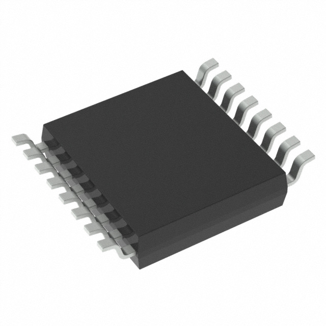
TMUX1309QPWRQ1
ActiveAUTOMOTIVE 5-V, 4:1, TWO-CHANNEL MULTIPLEXER WITH INJECTION CONTROL AND 1.8-V LOGIC
Deep-Dive with AI
Search across all available documentation for this part.

TMUX1309QPWRQ1
ActiveAUTOMOTIVE 5-V, 4:1, TWO-CHANNEL MULTIPLEXER WITH INJECTION CONTROL AND 1.8-V LOGIC
Deep-Dive with AI
Technical Specifications
Parameters and characteristics for this part
| Specification | TMUX1309QPWRQ1 |
|---|---|
| -3db Bandwidth | 500 MHz |
| Channel Capacitance (CS(off), CD(off)) [custom] | 7 pF |
| Channel Capacitance (CS(off), CD(off)) [custom] | 14 pF |
| Charge Injection | -6.5 pC |
| Crosstalk | -90 dB |
| Current - Leakage (IS(off)) (Max) | 1 nA |
| Grade | Automotive |
| Mounting Type | Surface Mount |
| Multiplexer/Demultiplexer Circuit | 4:1 |
| Number of Circuits | 2 |
| On-State Resistance (Max) [Max] | 195 Ohm |
| Operating Temperature [Max] | 125 °C |
| Operating Temperature [Min] | -40 °C |
| Package / Case | 16-TSSOP |
| Package / Case [x] | 0.173 in |
| Package / Case [y] | 4.4 mm |
| Qualification | AEC-Q100 |
| Supplier Device Package | 16-TSSOP |
| Switch Circuit | SP4T |
| Switch Time (Ton, Toff) (Max) [custom] | 32 ns |
| Switch Time (Ton, Toff) (Max) [custom] | 40 ns |
| Voltage - Supply, Single (V+) [Max] | 5.5 V |
| Voltage - Supply, Single (V+) [Min] | 1.62 V |
Pricing
Prices provided here are for design reference only. For realtime values and availability, please visit the distributors directly
| Distributor | Package | Quantity | $ | |
|---|---|---|---|---|
| Digikey | Cut Tape (CT) | 1 | $ 0.35 | |
| 10 | $ 0.30 | |||
| 25 | $ 0.28 | |||
| 100 | $ 0.23 | |||
| 250 | $ 0.21 | |||
| 500 | $ 0.18 | |||
| 1000 | $ 0.14 | |||
| Digi-Reel® | 1 | $ 0.35 | ||
| 10 | $ 0.30 | |||
| 25 | $ 0.28 | |||
| 100 | $ 0.23 | |||
| 250 | $ 0.21 | |||
| 500 | $ 0.18 | |||
| 1000 | $ 0.14 | |||
| Tape & Reel (TR) | 2000 | $ 0.14 | ||
| Texas Instruments | LARGE T&R | 1 | $ 0.31 | |
| 100 | $ 0.21 | |||
| 250 | $ 0.16 | |||
| 1000 | $ 0.11 | |||
Description
General part information
TMUX1309-Q1 Series
The TMUX1308-Q1 and TMUX1309-Q1 are general purpose complementary metal-oxide semiconductor (CMOS) multiplexers (MUX). The TMUX1308-Q1 is an 8:1, 1-channel (single-ended) mux, while the TMUX1309-Q1 is a 4:1, 2-channel (differential) mux. The devices support bidirectional analog and digital signals on the source (Sx) and drain (Dx) pins ranging from GND to V DD.
The TMUX13xx-Q1 devices have an internal injection current control feature which eliminates the need for external diode and resistor networks typically used to protect the switch and keep the input signals within the supply voltage. The internal injection current control circuitry allows signals on disabled signal paths to exceed the supply voltage without affecting the signal of the enabled signal path. Additionally, the TMUX13xx-Q1 devices do not have an internal diode path to the supply pin, which eliminates the risk of damaging components connected to the supply pin or providing unintended power to the supply rail.
All logic inputs have 1.8 V logic compatible thresholds, ensuring both TTL and CMOS logic compatibility when operating with a valid supply voltage. Fail-Safe Logic circuitry allows voltages on the control pins to be applied before the supply pin, protecting the device from potential damage.
Documents
Technical documentation and resources


