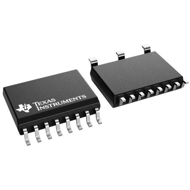
TPSI2072QDWQRQ1
ActiveAUTOMOTIVE, TWO-CHANNEL 600-V 50-MA ISOLATED SWITCH WITH 2-MA AVALANCHE RATING
Deep-Dive with AI
Search across all available documentation for this part.

TPSI2072QDWQRQ1
ActiveAUTOMOTIVE, TWO-CHANNEL 600-V 50-MA ISOLATED SWITCH WITH 2-MA AVALANCHE RATING
Technical Specifications
Parameters and characteristics for this part
| Specification | TPSI2072QDWQRQ1 |
|---|---|
| Approval Agency | UL, CSA, CQC, TUV, VDE |
| Circuit | DPST-NO (2 Form A) |
| Grade | Automotive |
| Load Current | 50 mA |
| Mounting Type | Surface Mount |
| On-State Resistance (Max) [Max] | 150 Ohm |
| Operating Temperature [Max] | 125 °C |
| Operating Temperature [Min] | -40 C |
| Output Type | DC |
| Package / Case | 0.295 " |
| Package / Case | 11-SOIC |
| Package / Case [y] | 7.5 mm |
| Qualification | AEC-Q100 |
| Supplier Device Package | 11-SOIC |
| Termination Style | Gull Wing |
| Voltage - Input [Max] | 20 V |
| Voltage - Input [Min] | 4.5 V |
| Voltage - Load [Max] | 600 V |
| Voltage - Load [Min] | 0 V |
Pricing
Prices provided here are for design reference only. For realtime values and availability, please visit the distributors directly
| Distributor | Package | Quantity | $ | |
|---|---|---|---|---|
| Digikey | N/A | 0 | $ 3.12 | |
| Tape & Reel (TR) | 2000 | $ 4.27 | ||
| Texas Instruments | LARGE T&R | 1 | $ 4.02 | |
| 100 | $ 3.52 | |||
| 250 | $ 2.47 | |||
| 1000 | $ 1.99 | |||
Description
General part information
TPSI2072-Q1 Series
The TPSI2072-Q1 is a two channel isolated solid state relay designed for high voltage automotive and industrial applications. The TPSI2072-Q1 uses TI’s high reliability capacitive isolation technology in combination with internal back-to-back MOSFETs to form a completely integrated solution requiring no secondary side power supply. The TPSI2072-Q1 improves system reliability as TI’s capacitive isolation technology does not suffer from mechanical wearout or photo degradation failure modes common in mechanical relay and photo relay components.
The primary side of the device is powered by only 9 mA of input current and incorporates fail-safe EN1 and EN2 pins preventing any possibility of back powering the VDD supply. In most applications, the VDD pin of the device should be connected to a system supply between 4.5 V–20 V and the EN1 and EN2 pins of the device should be driven by a GPIO output with logic HI between 2.1 V–20 V. In other applications, the VDD, EN1, and EN2 pins could be driven together directly from the system supply or from a GPIO output.
Each channel on the secondary side consists of back-to-back MOSFETs with a standoff voltage of +/-600 V from SM to S1 and SM to S2. The TPSI2072-Q1 MOSFET’s avalanche robustness and thermally conscious package design allow it to robustly support system level dielectric withstand testing (HiPot) and DC fast charger surge currents of up to 2 mA without requiring any external components.
Documents
Technical documentation and resources


