87946AYI-147LF/W
Obsolete1-TO-10 LOW SKEW,÷1,÷2 LVCMOS/LVTTL 2.5V, 3.3V FANOUT BUFFER
Deep-Dive with AI
Search across all available documentation for this part.

87946AYI-147LF/W
Obsolete1-TO-10 LOW SKEW,÷1,÷2 LVCMOS/LVTTL 2.5V, 3.3V FANOUT BUFFER
Deep-Dive with AI
Technical Specifications
Parameters and characteristics for this part
| Specification | 87946AYI-147LF/W |
|---|---|
| Differential - Input:Output | False |
| Frequency - Max [Max] | 250 MHz |
| Input | LVCMOS, LVTTL |
| Mounting Type | Surface Mount |
| Number of Circuits | 1 |
| Operating Temperature [Max] | 85 °C |
| Operating Temperature [Min] | -40 °C |
| Output | LVCMOS, LVTTL |
| Package / Case | 32-LQFP |
| Ratio - Input:Output [custom] | 1:10 |
| Supplier Device Package | 32-TQFP (7x7) |
| Type | Fanout Buffer (Distribution) |
| Voltage - Supply [Max] | 2.625 V, 3.465 V |
| Voltage - Supply [Min] | 2.375 V, 3.135 V |
Pricing
Prices provided here are for design reference only. For realtime values and availability, please visit the distributors directly
| Distributor | Package | Quantity | $ | |
|---|---|---|---|---|
Description
General part information
87946I-147 Series
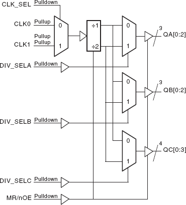
The 87946I-147 is a low skew, ÷1, ÷2 LVCMOS/LVTTL Fanout Buffer. The 87946I-147 has two selectable single-ended clock inputs. The single-ended clock inputs accept LVCMOS or LVTTL input levels. The low impedance LVCMOS/LVTTL outputs are designed to drive 50Ω series or parallel terminated transmission lines. The effective fanout can be increased from 10 to 20 by utilizing the ability of the outputs to drive two series terminated lines.
The divide select inputs, DIV_SELx, control the output frequency of each bank. The outputs can be utilized in the ÷1, ÷2 or a combination of ÷1 and ÷2 modes. The master reset input, MR/nOE, resets the internal frequency dividers and also controls the active and high impedance states of all outputs.
The 87946I-147 is characterized at full 3.3V for input VDD, and mixed 3.3V and 2.5V for output operating supply mode. Guaranteed bank, output and part-to-part skew characteristics make the 87946I-147 ideal for those clock distribution applications demanding well defined performance and repeatability.
Documents
Technical documentation and resources


