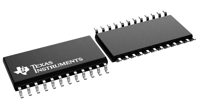
CD74HCT652M
ActiveHIGH SPEED CMOS LOGIC OCTAL BUS TRANSCEIVERS/REGISTERS WITH 3-STATE OUTPUTS
Deep-Dive with AI
Search across all available documentation for this part.

CD74HCT652M
ActiveHIGH SPEED CMOS LOGIC OCTAL BUS TRANSCEIVERS/REGISTERS WITH 3-STATE OUTPUTS
Deep-Dive with AI
Technical Specifications
Parameters and characteristics for this part
| Specification | CD74HCT652M |
|---|---|
| Current - Output High, Low [custom] | 6 mA |
| Current - Output High, Low [custom] | 6 mA |
| Mounting Type | Surface Mount |
| Number of Bits per Element | 8 |
| Number of Elements | 1 |
| Operating Temperature [Max] | 125 °C |
| Operating Temperature [Min] | -55 °C |
| Output Type | 3-State |
| Package / Case | 24-SOIC |
| Package / Case [custom] | 7.5 mm |
| Package / Case [custom] | 0.295 in |
| Supplier Device Package | 24-SOIC |
| Voltage - Supply [Max] | 5.5 V |
| Voltage - Supply [Min] | 4.5 V |
Pricing
Prices provided here are for design reference only. For realtime values and availability, please visit the distributors directly
| Distributor | Package | Quantity | $ | |
|---|---|---|---|---|
| Digikey | Tube | 325 | $ 2.94 | |
| Texas Instruments | TUBE | 1 | $ 3.50 | |
| 100 | $ 3.07 | |||
| 250 | $ 2.15 | |||
| 1000 | $ 1.73 | |||
Description
General part information
SN74HCT652 Series
The CD74HC652 and CD74HCT652 three-state, octal-bus transceiver/registers use silicon-gate CMOS technology to achieve operating speeds similar to LSTTL with the low power consumption of standard CMOS integrated circuits. The CD74HC652 and CD74HCT652 have non-inverting outputs. These devices consists of bus transceiver circuits, D-type flip-flops, and control circuitry arranged for multiplexed transmission of data directly from the data bus or from the internal storage registers. Output Enables OEABand OEBAare provided to control the transceiver functions. SAB and SBA control pins are provided to select whether real-time or stored data is transferred. The circuitry used for select control will eliminate the typical decoding glitch that occurs in a multiplexer during the transition between stored and real-time data. A LOW input level selects real-time data, and a HIGH selects stored data. The following examples demonstrates the four fundamentals bus-management functions that can be performed with the octal-bus transceivers and registers.
Data on the A or B data bus, or both, can be stored in the internal D flip-flops by low-to-high transitions at the appropriate clock pins (CAB or CBA) regardless of the select of the control pins. When SAB and SBA are in the real-time transfer mode, it is also possible to store data without using the D-type flip-flops by simultaneously enabling OEABand OEBA. In this configuration, each output reinforces its input. Thus, when all other data sources to the two sets of bus lines are at high impedance, each set of bus lines will remain at its last state.
The CD74HC652 and CD74HCT652 three-state, octal-bus transceiver/registers use silicon-gate CMOS technology to achieve operating speeds similar to LSTTL with the low power consumption of standard CMOS integrated circuits. The CD74HC652 and CD74HCT652 have non-inverting outputs. These devices consists of bus transceiver circuits, D-type flip-flops, and control circuitry arranged for multiplexed transmission of data directly from the data bus or from the internal storage registers. Output Enables OEABand OEBAare provided to control the transceiver functions. SAB and SBA control pins are provided to select whether real-time or stored data is transferred. The circuitry used for select control will eliminate the typical decoding glitch that occurs in a multiplexer during the transition between stored and real-time data. A LOW input level selects real-time data, and a HIGH selects stored data. The following examples demonstrates the four fundamentals bus-management functions that can be performed with the octal-bus transceivers and registers.
Documents
Technical documentation and resources


