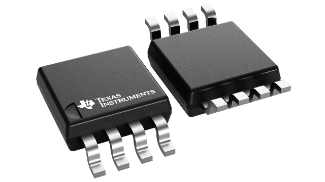
TMUX6219DGKRQ1
ActiveANALOG SWITCH/ANALOG MULTIPLEXER SINGLE 2:1 8-PIN VSSOP T/R AUTOMOTIVE AEC-Q100
Deep-Dive with AI
Search across all available documentation for this part.

TMUX6219DGKRQ1
ActiveANALOG SWITCH/ANALOG MULTIPLEXER SINGLE 2:1 8-PIN VSSOP T/R AUTOMOTIVE AEC-Q100
Technical Specifications
Parameters and characteristics for this part
| Specification | TMUX6219DGKRQ1 |
|---|---|
| -3db Bandwidth | 42 MHz |
| Channel Capacitance (CS(off), CD(off)) [custom] | 38 pF |
| Channel Capacitance (CS(off), CD(off)) [custom] | 38 pF |
| Channel-to-Channel Matching (ΔRon) | 80 mOhm |
| Charge Injection | -6 pC |
| Crosstalk | -106 dB |
| Current - Leakage (IS(off)) (Max) | 100 pA |
| Grade | Automotive |
| Mounting Type | Surface Mount |
| Multiplexer/Demultiplexer Circuit | 2:1 |
| Number of Circuits | 1 |
| On-State Resistance (Max) [Max] | 6.2 Ohm |
| Operating Temperature [Max] | 125 °C |
| Operating Temperature [Min] | -40 °C |
| Package / Case | 8-MSOP, 8-TSSOP |
| Package / Case | 3 mm |
| Package / Case [custom] | 0.118 in |
| Qualification | AEC-Q100 |
| Switch Circuit | SPDT |
| Switch Time (Ton, Toff) (Max) [custom] | 210 ns |
| Switch Time (Ton, Toff) (Max) [custom] | 180 ns |
| Voltage - Supply, Dual (V±) [Max] | 18 V |
| Voltage - Supply, Dual (V±) [Min] | -4.5 V |
| Voltage - Supply, Single (V+) [Max] | 36 V |
| Voltage - Supply, Single (V+) [Min] | 4.5 V |
Pricing
Prices provided here are for design reference only. For realtime values and availability, please visit the distributors directly
| Distributor | Package | Quantity | $ | |
|---|---|---|---|---|
| Digikey | Cut Tape (CT) | 1 | $ 4.64 | |
| 10 | $ 4.16 | |||
| 25 | $ 3.94 | |||
| 100 | $ 3.41 | |||
| 250 | $ 3.24 | |||
| 500 | $ 2.90 | |||
| 1000 | $ 2.45 | |||
| Digi-Reel® | 1 | $ 4.64 | ||
| 10 | $ 4.16 | |||
| 25 | $ 3.94 | |||
| 100 | $ 3.41 | |||
| 250 | $ 3.24 | |||
| 500 | $ 2.90 | |||
| 1000 | $ 2.45 | |||
| Tape & Reel (TR) | 2500 | $ 2.33 | ||
| Texas Instruments | LARGE T&R | 1 | $ 3.35 | |
| 100 | $ 2.94 | |||
| 250 | $ 2.06 | |||
| 1000 | $ 1.66 | |||
Description
General part information
TMUX6219-Q1 Series
The TMUX6219-Q1 is a complementary metal-oxide semiconductor (CMOS) switch in a single channel, 2:1 (SPDT) configuration. The device works with single supply (4.5V to 36V), dual supplies (±4.5V to ±18V), or asymmetric supplies (such as VDD = 5V, VSS = −8V). The TMUX6219-Q1 supports bidirectional analog and digital signals on the source (Sx) and drain (D) pins ranging from VSS to VDD.
The TMUX6219-Q1 can be enabled or disabled by controlling the EN pin. When disabled, both signal path switches are off. When enabled, the SEL pin can be used to turn on signal path 1 (S1 to D) or signal path 2 (S2 to D). All logic control inputs support logic levels from 1.8V to VDD, ensuring both TTL and CMOS logic compatibility when operating in the valid supply voltage range. Fail-Safe Logic circuitry allows voltages on the control pins to be applied before the supply pin, protecting the device from potential damage.
The TMUX6219-Q1 is part of the precision switches and multiplexers family of devices. These devices have very low on and off leakage currents and low charge injection, allowing them to be used in high precision measurement applications.
Documents
Technical documentation and resources


