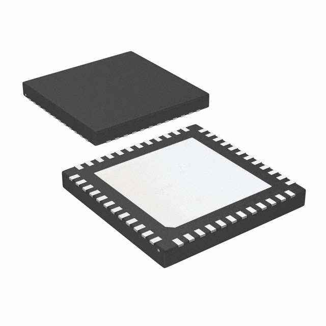
LMK03200ISQX/NOPB
ActivePRECISION 0-DELAY CLOCK CONDITIONER WITH INTEGRATED VCO
Deep-Dive with AI
Search across all available documentation for this part.

LMK03200ISQX/NOPB
ActivePRECISION 0-DELAY CLOCK CONDITIONER WITH INTEGRATED VCO
Technical Specifications
Parameters and characteristics for this part
| Specification | LMK03200ISQX/NOPB |
|---|---|
| Differential - Input:Output [custom] | True |
| Differential - Input:Output [custom] | True |
| Divider/Multiplier | Yes/No |
| Frequency - Max [Max] | 1.296 GHz |
| Input | LVDS, LVCMOS, LVPECL |
| Mounting Type | Surface Mount |
| Number of Circuits | 1 |
| Operating Temperature [Max] | 85 °C |
| Operating Temperature [Min] | -40 °C |
| Output | LVPECL, LVDS |
| Package / Case | 48-WFQFN Exposed Pad |
| PLL | False |
| Ratio - Input:Output | 1:8 |
| Supplier Device Package | 48-WQFN (7x7) |
| Type | Clock Conditioner |
| Voltage - Supply [Max] | 3.45 V |
| Voltage - Supply [Min] | 3.15 V |
Pricing
Prices provided here are for design reference only. For realtime values and availability, please visit the distributors directly
| Distributor | Package | Quantity | $ | |
|---|---|---|---|---|
| Digikey | Tape & Reel (TR) | 2500 | $ 9.67 | |
| Texas Instruments | LARGE T&R | 1 | $ 12.42 | |
| 100 | $ 10.85 | |||
| 250 | $ 8.36 | |||
| 1000 | $ 7.48 | |||
Description
General part information
LMK03200 Series
The LMK03200 family of precision clock conditioners combine the functions of jitter cleaning/reconditioning, multiplication, and 0-delay distribution of a reference clock. The devices integrate a Voltage Controlled Oscillator (VCO), a high performance Integer-N Phase Locked Loop (PLL), a partially integrated loop filter, and up to eight outputs in various LVDS and LVPECL combinations.
The VCO output is optionally accessible on the Fout port. Internally, the VCO output goes through a VCO divider to feed the various clock distribution blocks.
Each clock distribution block includes a programmable divider, a phase synchronization circuit, a programmable delay, a clock output mux, and an LVDS or LVPECL output buffer. The PLL also features delay blocks to permit global phase adjustment of clock output phase. This allows multiple integer-related and phase-adjusted copies of the reference to be distributed to eight system components.


