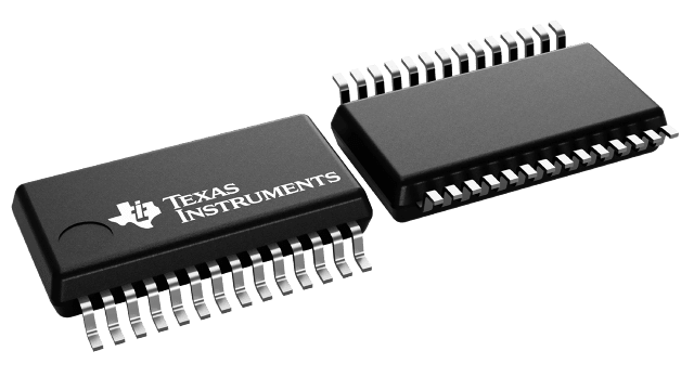
CDC2536DB
Active125-MHZ, 3.3-V PLL CLOCK DRIVER WITH 1/2X, 1X AND 2X FREQUENCY OPTIONS
Deep-Dive with AI
Search across all available documentation for this part.

CDC2536DB
Active125-MHZ, 3.3-V PLL CLOCK DRIVER WITH 1/2X, 1X AND 2X FREQUENCY OPTIONS
Technical Specifications
Parameters and characteristics for this part
| Specification | CDC2536DB |
|---|---|
| Differential - Input:Output | False |
| Mounting Type | Surface Mount |
| Number of Circuits | 1 |
| Operating Temperature [Max] | 70 °C |
| Operating Temperature [Min] | 0 °C |
| Output | LVTTL |
| Package / Case | 28-SSOP |
| Package / Case [custom] | 0.209 in |
| Package / Case [custom] | 5.3 mm |
| PLL | Yes with Bypass |
| Ratio - Input:Output [custom] | 1:6 |
| Supplier Device Package | 28-SSOP |
| Type | PLL Clock Driver |
| Voltage - Supply [Max] | 3.6 V |
| Voltage - Supply [Min] | 3 V |
Pricing
Prices provided here are for design reference only. For realtime values and availability, please visit the distributors directly
| Distributor | Package | Quantity | $ | |
|---|---|---|---|---|
| Digikey | Tube | 150 | $ 8.97 | |
| Texas Instruments | TUBE | 1 | $ 9.18 | |
| 100 | $ 7.49 | |||
| 250 | $ 5.88 | |||
| 1000 | $ 4.99 | |||
Description
General part information
CDC2536 Series
The CDC2536 is a high-performance, low-skew, low-jitter clock driver. It uses a phase-lock loop (PLL) to precisely align, in both frequency and phase, the clock output signals to the clock input (CLKIN) signal. It is specifically designed for use with synchronous DRAMs and popular microprocessors operating at speeds from 50 MHz to 100 MHz or down to 25 MHz on outputs configured as half-frequency outputs. The CDC2536 operates at 3.3-V VCCand is designed to drive a 50-W transmission line. The CDC2536 also provides on-chip series-damping resistors, eliminating the need for external termination components.
The feedback (FBIN) input is used to synchronize the output clocks in frequency and phase to the input clock (CLKIN). One of the six output clocks must be fed back to FBIN for the PLL to maintain synchronization between CLKIN and the outputs. The output used as the feedback pin is synchronized to the same frequency as CLKIN.
The Y outputs can be configured to switch in phase and at the same frequency as CLKIN. The select (SEL) input configures three Y outputs to operate at one-half or double the CLKIN frequency, depending on which pin is fed back to FBIN (see Tables 1 and 2). All output signal duty cycles are adjusted to 50% independent of the duty cycle at the input clock.
Documents
Technical documentation and resources


