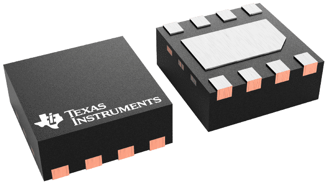
TPS62082DSGR
ActiveSWITCHING VOLTAGE REGULATORS 1.2A HIGH EFF STEP D OWN CONVERTER A 595-TPS62082DSGT
Deep-Dive with AI
Search across all available documentation for this part.

TPS62082DSGR
ActiveSWITCHING VOLTAGE REGULATORS 1.2A HIGH EFF STEP D OWN CONVERTER A 595-TPS62082DSGT
Technical Specifications
Parameters and characteristics for this part
| Specification | TPS62082DSGR |
|---|---|
| Current - Output | 1.2 A |
| Frequency - Switching | 2 MHz |
| Function | Step-Down |
| Mounting Type | Surface Mount |
| Number of Outputs | 1 |
| Operating Temperature [Max] | 125 °C |
| Operating Temperature [Min] | -40 C |
| Output Configuration | Positive |
| Package / Case | 8-WFDFN Exposed Pad |
| Supplier Device Package | 8-WSON (2x2) |
| Synchronous Rectifier | True |
| Topology | Buck |
| Voltage - Input (Max) [Max] | 6 V |
| Voltage - Input (Min) [Min] | 2.3 V |
| Voltage - Output (Min/Fixed) | 3.3 V |
Pricing
Prices provided here are for design reference only. For realtime values and availability, please visit the distributors directly
| Distributor | Package | Quantity | $ | |
|---|---|---|---|---|
| Digikey | Cut Tape (CT) | 1 | $ 1.64 | |
| 10 | $ 1.48 | |||
| 25 | $ 1.39 | |||
| 100 | $ 1.19 | |||
| 250 | $ 1.12 | |||
| 500 | $ 0.98 | |||
| 1000 | $ 0.81 | |||
| Digi-Reel® | 1 | $ 1.64 | ||
| 10 | $ 1.48 | |||
| 25 | $ 1.39 | |||
| 100 | $ 1.19 | |||
| 250 | $ 1.12 | |||
| 500 | $ 0.98 | |||
| 1000 | $ 0.81 | |||
| N/A | 11023 | $ 1.76 | ||
| Tape & Reel (TR) | 3000 | $ 0.75 | ||
| 6000 | $ 0.72 | |||
| Mouser | N/A | 1 | $ 1.55 | |
| 10 | $ 1.14 | |||
| 25 | $ 1.03 | |||
| 100 | $ 0.92 | |||
| 250 | $ 0.86 | |||
| 500 | $ 0.83 | |||
| 1000 | $ 0.80 | |||
| 3000 | $ 0.72 | |||
| 6000 | $ 0.72 | |||
| Texas Instruments | LARGE T&R | 1 | $ 1.24 | |
| 100 | $ 1.02 | |||
| 250 | $ 0.73 | |||
| 1000 | $ 0.55 | |||
Description
General part information
TPS62082 Series
The TPS6208x devices are a family of high frequency synchronous step down converters. With an input voltage range of 2.3 V to 6 V, common battery technologies are supported. Alternatively, the device can be used for low voltage system power rails.
The TPS6208x focuses on high efficiency step-down conversion over a wide output current range. At medium to heavy loads, the converter operates in PWM mode and automatically enters Power Save Mode operation at light load currents to maintain high efficiency over the entire load current range. To maintain high efficiency at very low load or no load currents, a Snooze Mode with an ultra-low quiescent current is implemented. This function, enabled by the MODE pin, increases the run-time of battery driven applications and keeps the standby current at its lowest level to meet green energy standards targeting a low stand-by current.
To address the requirements of system power rails, the internal loop compensation allows a large selection of external output capacitor values in excess of 100 µF. With its DCS-Control™ architecture, excellent load transient performance and output voltage regulation accuracy is achieved. The device is available in 2-mm × 2-mm WSON package with Thermal PAD.
Documents
Technical documentation and resources


