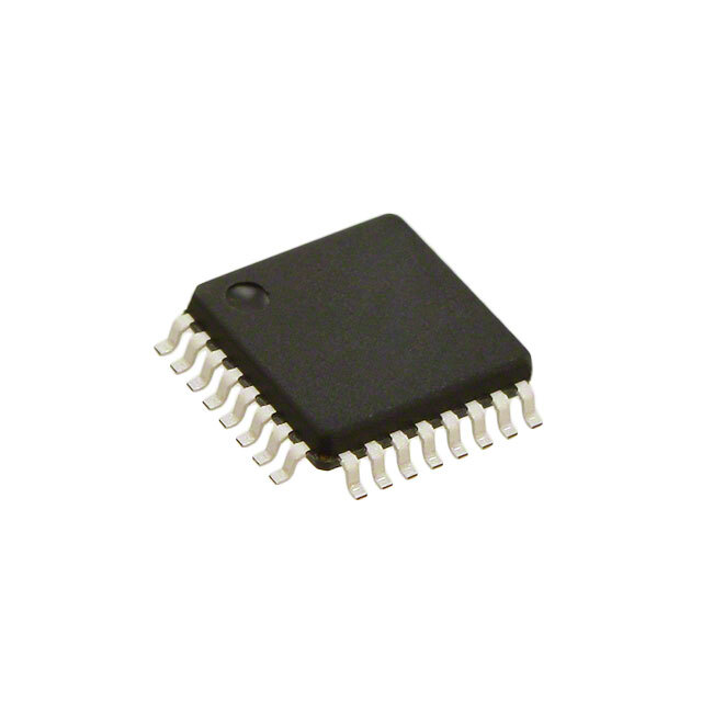
SCAN90CP02VY/NOPB
Active1.5-GBPS 2X2 LVDS CROSSPOINT SWITCH WITH PRE-EMPHASIS AND IEEE 1149.6
Deep-Dive with AI
Search across all available documentation for this part.

SCAN90CP02VY/NOPB
Active1.5-GBPS 2X2 LVDS CROSSPOINT SWITCH WITH PRE-EMPHASIS AND IEEE 1149.6
Technical Specifications
Parameters and characteristics for this part
| Specification | SCAN90CP02VY/NOPB |
|---|---|
| Circuit | 1 x 2:2 |
| Independent Circuits | 1 |
| Mounting Type | Surface Mount |
| Operating Temperature [Max] | 85 °C |
| Operating Temperature [Min] | -40 °C |
| Package / Case | 32-LQFP |
| Supplier Device Package | 32-TQFP (7x7) |
| Type | Crosspoint Switch |
| Voltage - Supply [Max] | 3.6 V |
| Voltage - Supply [Min] | 3 V |
| Voltage Supply Source | Single Supply |
Pricing
Prices provided here are for design reference only. For realtime values and availability, please visit the distributors directly
| Distributor | Package | Quantity | $ | |
|---|---|---|---|---|
| Digikey | Tray | 250 | $ 5.27 | |
| Texas Instruments | JEDEC TRAY (10+1) | 1 | $ 5.65 | |
| 100 | $ 4.60 | |||
| 250 | $ 3.62 | |||
| 1000 | $ 3.07 | |||
Description
General part information
SCAN90CP02 Series
The SCAN90CP02 is a 1.5 Gbps 2 x 2 LVDS crosspoint switch. High speed data paths and flow-through pinout minimize internal device jitter, while configurable 0/25/50/100% pre-emphasis overcomes external ISI jitter effects of lossy backplanes and cables. The differential inputs interface to LVDS and Bus LVDS signals such as those on TI's 10-, 16-, and 18- bit Bus LVDS SerDes, as well as CML and LVPECL. The SCAN90CP02 can also be used with ASICs and FPGAs. The non-blocking crosspoint architecture is pin-configurable as a 1:2 clock or data splitter, 2:1 redundancy mux, crossover function, or dual buffer for signal booster and stub hider applications.
Integrated IEEE 1149.1 (JTAG) and 1149.6 circuitry supports testability of both single-ended LVTTL/CMOS and differential LVDS PCB interconnect. The 3.3V supply, CMOS process, and LVDS I/O ensure high performance at low power over the entire industrial -40 to +85°C temperature range.
The SCAN90CP02 is a 1.5 Gbps 2 x 2 LVDS crosspoint switch. High speed data paths and flow-through pinout minimize internal device jitter, while configurable 0/25/50/100% pre-emphasis overcomes external ISI jitter effects of lossy backplanes and cables. The differential inputs interface to LVDS and Bus LVDS signals such as those on TI's 10-, 16-, and 18- bit Bus LVDS SerDes, as well as CML and LVPECL. The SCAN90CP02 can also be used with ASICs and FPGAs. The non-blocking crosspoint architecture is pin-configurable as a 1:2 clock or data splitter, 2:1 redundancy mux, crossover function, or dual buffer for signal booster and stub hider applications.


