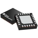
TPS65193RGER
Active5-CHANNEL LEVEL SHIFTER FOR LCD DISPLAYS (DUAL CHANNEL SCAN DRIVER)
Deep-Dive with AI
Search across all available documentation for this part.

TPS65193RGER
Active5-CHANNEL LEVEL SHIFTER FOR LCD DISPLAYS (DUAL CHANNEL SCAN DRIVER)
Technical Specifications
Parameters and characteristics for this part
| Specification | TPS65193RGER |
|---|---|
| Applications | TFT-LCD Panels: Scan Driver |
| Current - Supply | 600 µA |
| Mounting Type | Surface Mount |
| Number of Circuits | 2 |
| Package / Case | 24-VFQFN Exposed Pad |
| Slew Rate | 55 V/µs |
| Supplier Device Package | 24-VQFN (4x4) |
Pricing
Prices provided here are for design reference only. For realtime values and availability, please visit the distributors directly
| Distributor | Package | Quantity | $ | |
|---|---|---|---|---|
| Digikey | Cut Tape (CT) | 1 | $ 2.10 | |
| Digi-Reel® | 1 | $ 2.10 | ||
| Tape & Reel (TR) | 3000 | $ 0.96 | ||
| 6000 | $ 0.92 | |||
| Texas Instruments | LARGE T&R | 1 | $ 1.58 | |
| 100 | $ 1.30 | |||
| 250 | $ 0.94 | |||
| 1000 | $ 0.70 | |||
Description
General part information
TPS65193 Series
The TPS65193 is dual high-voltage scan driver to drive an amorphous-silicon-gate (ASG) circuit on TFT glass. Each single high-voltage scan driver receives logic-level inputs of CPVx and generates two high-voltage outputs of CKVx and CKVBx. The device receives a logic-level input of STV and generates a high-voltage output of STVP. These outputs are swings from Voff (–28 V) to Von (35 V) and are used to drive the ASG circuit and charge/discharge the capacitive loads of the TFT LCD. In order to reduce the power dissipation of the device, a charge-share function is implemented. The device features a discharge function, which shorts Voff to GND in order to shut down the panel faster when the LCD is turned off.
The TPS65193 is dual high-voltage scan driver to drive an amorphous-silicon-gate (ASG) circuit on TFT glass. Each single high-voltage scan driver receives logic-level inputs of CPVx and generates two high-voltage outputs of CKVx and CKVBx. The device receives a logic-level input of STV and generates a high-voltage output of STVP. These outputs are swings from Voff (–28 V) to Von (35 V) and are used to drive the ASG circuit and charge/discharge the capacitive loads of the TFT LCD. In order to reduce the power dissipation of the device, a charge-share function is implemented. The device features a discharge function, which shorts Voff to GND in order to shut down the panel faster when the LCD is turned off.


