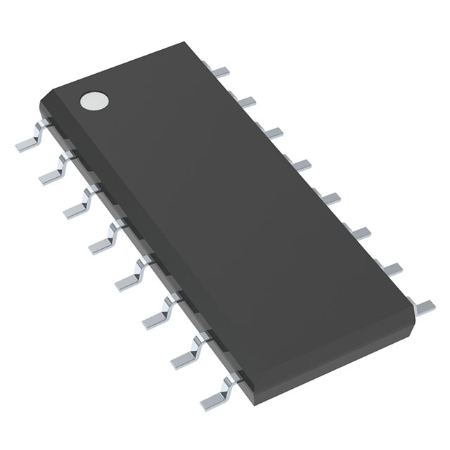
SN74LS174DR
ActiveFLIP FLOP D-TYPE BUS INTERFACE POS-EDGE PUSH-PULL 1-ELEMENT 16-PIN SOIC T/R
Deep-Dive with AI
Search across all available documentation for this part.

SN74LS174DR
ActiveFLIP FLOP D-TYPE BUS INTERFACE POS-EDGE PUSH-PULL 1-ELEMENT 16-PIN SOIC T/R
Deep-Dive with AI
Technical Specifications
Parameters and characteristics for this part
| Specification | SN74LS174DR |
|---|---|
| Clock Frequency | 40 MHz |
| Current - Output High, Low [custom] | 400 µA |
| Current - Output High, Low [custom] | 8 mA |
| Current - Quiescent (Iq) | 26 mA |
| Max Propagation Delay @ V, Max CL | 30 ns |
| Mounting Type | Surface Mount |
| Number of Bits per Element | 6 |
| Number of Elements | 1 |
| Operating Temperature [Max] | 70 °C |
| Operating Temperature [Min] | 0 °C |
| Output Type | Non-Inverted |
| Package / Case | 16-SOIC |
| Package / Case [x] | 0.154 in |
| Package / Case [y] | 3.9 mm |
| Supplier Device Package | 16-SOIC |
| Trigger Type | Positive Edge |
| Type | D-Type |
| Voltage - Supply [Max] | 5.25 V |
| Voltage - Supply [Min] | 4.75 V |
Pricing
Prices provided here are for design reference only. For realtime values and availability, please visit the distributors directly
| Distributor | Package | Quantity | $ | |
|---|---|---|---|---|
| Digikey | Cut Tape (CT) | 1 | $ 0.91 | |
| 10 | $ 0.81 | |||
| 25 | $ 0.77 | |||
| 100 | $ 0.63 | |||
| 250 | $ 0.59 | |||
| 500 | $ 0.52 | |||
| 1000 | $ 0.41 | |||
| Digi-Reel® | 1 | $ 0.91 | ||
| 10 | $ 0.81 | |||
| 25 | $ 0.77 | |||
| 100 | $ 0.63 | |||
| 250 | $ 0.59 | |||
| 500 | $ 0.52 | |||
| 1000 | $ 0.41 | |||
| Tape & Reel (TR) | 2500 | $ 0.34 | ||
| Texas Instruments | LARGE T&R | 1 | $ 0.74 | |
| 100 | $ 0.57 | |||
| 250 | $ 0.42 | |||
| 1000 | $ 0.30 | |||
Description
General part information
SN74LS174 Series
These monolithic, positive-edge-triggered flip-flops utilize TTL circuitry to implement D-type flip-flop logic. All have a direct clear input, and the '175, 'LS175, and 'S175 feature complementary outputs from each flip-flop.
Information at the D inputs meeting the setup time requirements is transferred to the Q outputs on the positive-going edge of the clock pulse. Clock triggering occurs at a particular voltage level and is not directly related to the transition time of the positive-going pulse. When the clock input is at either the high or low level, the D input signal has no effect at the output.
These circuits are fully compatible for use with most TTL circuits.
Documents
Technical documentation and resources


