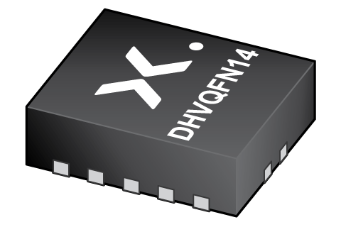
NXB0104BQ-Q100X
ActiveDUAL SUPPLY TRANSLATING TRANSCEIVER; AUTO DIRECTION SENSING; 3-STATE
Deep-Dive with AI
Search across all available documentation for this part.

NXB0104BQ-Q100X
ActiveDUAL SUPPLY TRANSLATING TRANSCEIVER; AUTO DIRECTION SENSING; 3-STATE
Technical Specifications
Parameters and characteristics for this part
| Specification | NXB0104BQ-Q100X |
|---|---|
| Channel Type | Bidirectional |
| Channels per Circuit | 4 |
| Data Rate | 100 Mbps |
| Grade | Automotive |
| Mounting Type | Surface Mount |
| Number of Circuits | 1 |
| Operating Temperature [Max] | 125 °C |
| Operating Temperature [Min] | -40 °C |
| Output Type | Tri-State |
| Package / Case | 14-VFQFN Exposed Pad |
| Qualification | AEC-Q100 |
| Supplier Device Package | 14-DHVQFN (2.5x3) |
| Translator Type | Voltage Level |
| Voltage - VCCA [Max] | 3.6 V |
| Voltage - VCCA [Min] | 1.2 V |
| Voltage - VCCB [Max] | 5.5 V |
| Voltage - VCCB [Min] | 1.65 V |
Pricing
Prices provided here are for design reference only. For realtime values and availability, please visit the distributors directly
| Distributor | Package | Quantity | $ | |
|---|---|---|---|---|
| Digikey | Cut Tape (CT) | 1 | $ 0.86 | |
| 10 | $ 0.76 | |||
| 25 | $ 0.71 | |||
| 100 | $ 0.58 | |||
| 250 | $ 0.54 | |||
| 500 | $ 0.46 | |||
| 1000 | $ 0.37 | |||
| Digi-Reel® | 1 | $ 0.86 | ||
| 10 | $ 0.76 | |||
| 25 | $ 0.71 | |||
| 100 | $ 0.58 | |||
| 250 | $ 0.54 | |||
| 500 | $ 0.46 | |||
| 1000 | $ 0.37 | |||
| N/A | 6 | $ 0.91 | ||
| Tape & Reel (TR) | 3000 | $ 0.33 | ||
| 6000 | $ 0.31 | |||
| 15000 | $ 0.30 | |||
| 30000 | $ 0.29 | |||
Description
General part information
NXB0104 Series
The NXB0104-Q100 is a 4-bit, dual supply translating transceiver with auto direction sensing, that enables bidirectional voltage level translation. It features two 4-bit input-output ports (An and Bn), one output enable input (OE) and two supply pins (VCC(A)and VCC(B)). VCC(A)can be supplied at any voltage between 1.2 V and 3.6 V and VCC(B)can be supplied at any voltage between 1.65 V and 5.5 V, making the device suitable for translating between any of the low voltage nodes (1.2 V, 1.5 V, 1.8 V, 2.5 V, 3.3 V and 5.0 V). Pins An and OE are referenced to VCC(A)and pins Bn are referenced to VCC(B). A LOW level at pin OE causes the outputs to assume a high-impedance OFF-state. This device is fully specified for partial power-down applications using IOFF. The IOFFcircuitry disables the output, preventing the damaging backflow current through the device when it is powered down.
Documents
Technical documentation and resources


