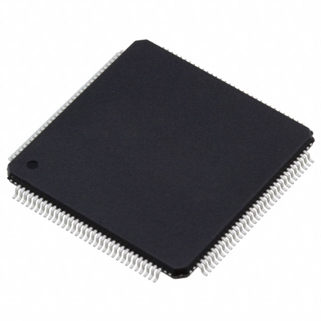
ADC081500CIYB/NOPB
Active8-BIT, 1.5-GSPS ANALOG-TO-DIGITAL CONVERTER (ADC)
Deep-Dive with AI
Search across all available documentation for this part.

ADC081500CIYB/NOPB
Active8-BIT, 1.5-GSPS ANALOG-TO-DIGITAL CONVERTER (ADC)
Technical Specifications
Parameters and characteristics for this part
| Specification | ADC081500CIYB/NOPB |
|---|---|
| Architecture | Folding Interpolating |
| Configuration | S/H-ADC |
| Data Interface | LVDS - Parallel |
| Input Type | Differential |
| Mounting Type | Surface Mount |
| Number of A/D Converters | 1 |
| Number of Bits | 8 |
| Number of Inputs | 1 |
| Operating Temperature [Max] | 85 °C |
| Operating Temperature [Min] | -40 °C |
| Ratio - S/H:ADC | 1:1 |
| Reference Type | Internal |
| Sampling Rate (Per Second) | 1.5 G |
| Supplier Device Package | 128-HLQFP (20x20) |
| Voltage - Supply, Analog [Max] | 2 V |
| Voltage - Supply, Analog [Min] | 1.8 V |
| Voltage - Supply, Digital [Max] | 2 V |
| Voltage - Supply, Digital [Min] | 1.8 V |
Pricing
Prices provided here are for design reference only. For realtime values and availability, please visit the distributors directly
| Distributor | Package | Quantity | $ | |
|---|---|---|---|---|
| Digikey | Tray | 2 | $ 396.27 | |
| 10 | $ 384.36 | |||
| 26 | $ 381.38 | |||
| Texas Instruments | JEDEC TRAY (10+1) | 1 | $ 342.20 | |
| 100 | $ 309.75 | |||
| 250 | $ 300.90 | |||
| 1000 | $ 295.00 | |||
Description
General part information
ADC081500 Series
The ADC081500 is a low power, high performance CMOS analog-to-digital converter that digitizes signals to 8 bits resolution at sample rates up to 1.7 GSPS. Consuming a typical 1.2 W at 1.5 GSPS from a single 1.9 Volt supply, this device is ensured to have no missing codes over the full operating temperature range. The unique folding and interpolating architecture, the fully differential comparator design, the innovative design of the internal sample-and-hold amplifier and the self-calibration scheme enable a very flat response of all dynamic parameters beyond Nyquist, producing a high 7.3 ENOB with a 748 MHz input signal and a 1.5 GHz sample rate while providing a 10-18B.E.R. Output formatting is offset binary and the LVDS digital outputs are compatible with IEEE 1596.3-1996, with the exception of an adjustable output offset voltage between 0.8V and 1.2V.
The converter output has a 1:2 demultiplexer that feeds two LVDS buses and reduces the output data rate on each bus to one-half the sample rate.
The converter typically consumes less than 3.5 mW in the Power Down Mode and is available in a 128-lead, thermally enhanced exposed pad HLQFP and operates over the Industrial (-40°C ≤ TA≤ +85°C) temperature range.
Documents
Technical documentation and resources


