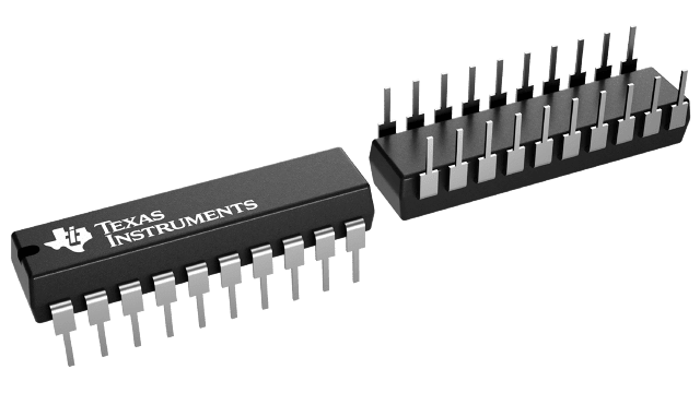
SN74F241N
Active8-CH, 4.5-V TO 5.5-V BIPOLAR BUFFERS WITH 3-STATE OUTPUTS
Deep-Dive with AI
Search across all available documentation for this part.

SN74F241N
Active8-CH, 4.5-V TO 5.5-V BIPOLAR BUFFERS WITH 3-STATE OUTPUTS
Deep-Dive with AI
Technical Specifications
Parameters and characteristics for this part
| Specification | SN74F241N |
|---|---|
| Current - Output High, Low [custom] | 64 mA |
| Current - Output High, Low [custom] | 15 mA |
| Logic Type | Buffer, Non-Inverting |
| Mounting Type | Through Hole |
| Number of Bits per Element | 4 |
| Number of Elements | 2 |
| Operating Temperature [Max] | 70 °C |
| Operating Temperature [Min] | 0 °C |
| Output Type | 3-State |
| Package / Case | 20-DIP |
| Package / Case | 7.62 mm |
| Package / Case | 0.3 in |
| Supplier Device Package | 20-PDIP |
| Voltage - Supply [Max] | 5.5 V |
| Voltage - Supply [Min] | 4.5 V |
Pricing
Prices provided here are for design reference only. For realtime values and availability, please visit the distributors directly
| Distributor | Package | Quantity | $ | |
|---|---|---|---|---|
| Digikey | Tube | 1 | $ 0.88 | |
| 20 | $ 0.79 | |||
| 40 | $ 0.75 | |||
| 100 | $ 0.61 | |||
| 260 | $ 0.57 | |||
| 500 | $ 0.51 | |||
| 1000 | $ 0.47 | |||
| Texas Instruments | TUBE | 1 | $ 1.21 | |
| 100 | $ 0.93 | |||
| 250 | $ 0.68 | |||
| 1000 | $ 0.49 | |||
Description
General part information
SN74F241 Series
These octal buffers and line drivers are designed specifically to improve both the performance and density of 3-state memory address drivers, clock drivers, and bus-oriented receivers and transmitters. Taken together with the ´F240 and ´F244, these devices provide the choice of selected combinations of inverting and non inverting outputs, symmetrical(active-low output-enable) inputs, and complementary OE andinputs.
The SN54F241 is characterized for operation over the full military temperature range of -55°C to 125°C. The SN74F241 is characterized for operation from 0°C to 70°C.
These octal buffers and line drivers are designed specifically to improve both the performance and density of 3-state memory address drivers, clock drivers, and bus-oriented receivers and transmitters. Taken together with the ´F240 and ´F244, these devices provide the choice of selected combinations of inverting and non inverting outputs, symmetrical(active-low output-enable) inputs, and complementary OE andinputs.
Documents
Technical documentation and resources


