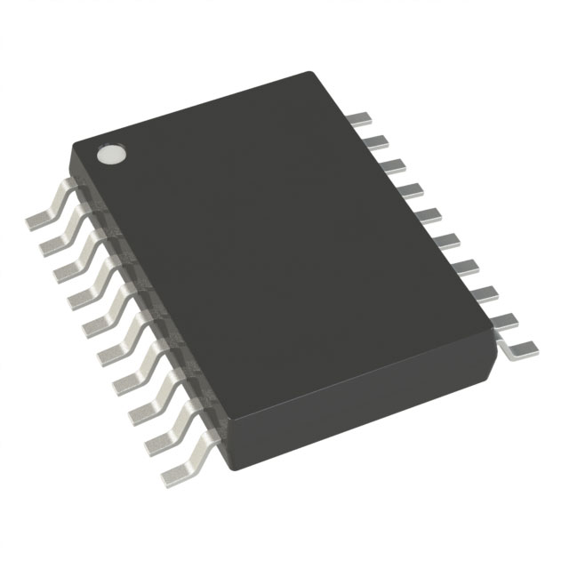
9DB202CGLFT
ObsoleteIC JITTER ATTENUATOR 20-TSSOP
Deep-Dive with AI
Search across all available documentation for this part.

9DB202CGLFT
ObsoleteIC JITTER ATTENUATOR 20-TSSOP
Deep-Dive with AI
Technical Specifications
Parameters and characteristics for this part
| Specification | 9DB202CGLFT |
|---|---|
| Differential - Input:Output [custom] | True |
| Differential - Input:Output [custom] | True |
| Frequency - Max [Max] | 140 MHz |
| Input | HCSL, LVPECL, SSTL, LVDS, LVHSTL |
| Main Purpose | PCI Express (PCIe) |
| Mounting Type | Surface Mount |
| Number of Circuits | 1 |
| Operating Temperature [Max] | 70 °C |
| Operating Temperature [Min] | 0 °C |
| Output | HCSL |
| Package / Case | 20-TSSOP |
| Package / Case [x] | 0.173 in |
| Package / Case [y] | 4.4 mm |
| PLL | True |
| Ratio - Input:Output [custom] | 1:2 |
| Supplier Device Package | 20-TSSOP |
| Voltage - Supply [Max] | 3.465 V |
| Voltage - Supply [Min] | 3.135 V |
Pricing
Prices provided here are for design reference only. For realtime values and availability, please visit the distributors directly
| Distributor | Package | Quantity | $ | |
|---|---|---|---|---|
Description
General part information
9DB202 Series
The 9DB202 is a high performance 1-to-2 Differential-to-HCSL Jitter Attenuator designed for use in PCI Express®™ systems. In some PCI Express®™ systems, such as those found in desktop PCs, the PCI Express®™ clocks are generated from a low bandwidth, high phase noise PLL frequency synthesizer. In these systems, a jitter-attenuating device may be necessary in order to reduce high frequency random and deterministic jitter components from the PLL synthesizer and from the system board. The 9DB202 has two PLL bandwidth modes. In low bandwidth mode, the PLL loop bandwidth is 500kHz. This setting offers the best jitter attenuation and is still high enough to pass a triangular input spread spectrum profile. In high bandwidth mode, the PLL bandwidth is at 1MHz and allows the PLL to pass more spread spectrum modulation. For serdes which have x10 reference multipliers instead of x12.5 multipliers, each of the two PCI Express®™ outputs (PCIEX0:1) can be set for 125MHz instead of 100MHz by configuring the appropriate frequency select pins (FS0:1).
Documents
Technical documentation and resources


