Zenode.ai Logo
Beta
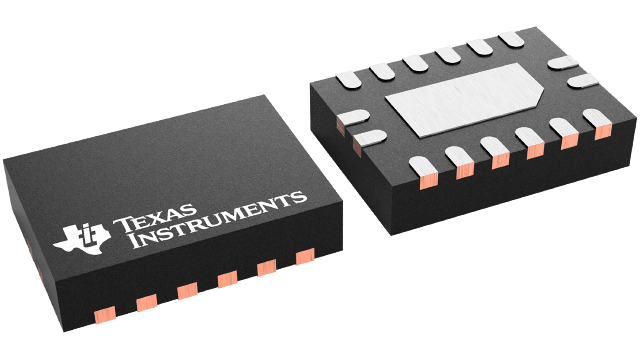
WQFN (BQB)
Integrated Circuits (ICs)

SN74LVC2G101BQBR

Active
Texas Instruments

TWO-CHANNEL 1.1V-TO-3.6V CONFIGURABLE GATE FOR CLOCK INPUT WITH SCHMITT-TRIGGER INPUTS

WQFN (BQB)
Integrated Circuits (ICs)

SN74LVC2G101BQBR

Active
Texas Instruments

TWO-CHANNEL 1.1V-TO-3.6V CONFIGURABLE GATE FOR CLOCK INPUT WITH SCHMITT-TRIGGER INPUTS

Technical Specifications

Parameters and characteristics for this part

SpecificationSN74LVC2G101BQBR
null

Pricing

Prices provided here are for design reference only. For realtime values and availability, please visit the distributors directly

DistributorPackageQuantity$
DigikeyTape & Reel (TR) 3000$ 0.39
6000$ 0.37
15000$ 0.36
Texas InstrumentsLARGE T&R 1$ 0.69
100$ 0.53
250$ 0.39
1000$ 0.28

Description

General part information

SN74LVC2G101 Series

The SN74LVC2G101 contains two independent D-type flip-flops. Each channel has data (D), clear (CLR), and clock (CLKA, CLKB, CLKC, CLKD) inputs and a non-inverted output (Q). The clock inputs can be configured for use in a wide variety of applications, allowing for configuration as 2-input AND, OR, NAND, NOR, XOR, XNOR, as well as 1-input inverted or non-inverted operation. All inputs include Schmitt-trigger architecture.

The SN74LVC2G101 contains two independent D-type flip-flops. Each channel has data (D), clear (CLR), and clock (CLKA, CLKB, CLKC, CLKD) inputs and a non-inverted output (Q). The clock inputs can be configured for use in a wide variety of applications, allowing for configuration as 2-input AND, OR, NAND, NOR, XOR, XNOR, as well as 1-input inverted or non-inverted operation. All inputs include Schmitt-trigger architecture.

Documents

Technical documentation and resources

Power-Up 3-State (PU3S) Circuits in TI Standard Logic Devices

Application note

SN74LVC2G101 Dual D-Type Flip-Flop with Configurable Multiple-Function Gated Clock datasheet

Data sheet

LOGIC Pocket Data Book (Rev. B)

User guide

Understanding Advanced Bus-Interface Products Design Guide

Application note

Implications of Slow or Floating CMOS Inputs (Rev. E)

Application note

Live Insertion

Application note

CMOS Power Consumption and CPD Calculation (Rev. B)

Application note

Semiconductor Packing Material Electrostatic Discharge (ESD) Protection

Application note

Selecting the Right Level Translation Solution (Rev. A)

Application note

Signal Switch Data Book (Rev. A)

User guide

STANDARD LINEAR AND LOGIC FOR DVD/VCD PLAYERS

More literature

Understanding and Interpreting Standard-Logic Data Sheets (Rev. C)

Application note

Use of the CMOS Unbuffered Inverter in Oscillator Circuits

Application note

16-Bit Widebus Logic Families in 56-Ball, 0.65-mm Pitch Very Thin Fine-Pitch BGA (Rev. B)

Application note

Bus-Interface Devices With Output-Damping Resistors Or Reduced-Drive Outputs (Rev. A)

Application note

Logic Guide (Rev. AB)

Selection guide

Low-Voltage Logic (LVC) Designer's Guide

Design guide

Design Summary for WCSP Little Logic (Rev. B)

Product overview

Input and Output Characteristics of Digital Integrated Circuits

Application note

LVC Characterization Information

Application note

Texas Instruments Little Logic Application Report

Application note

TI IBIS File Creation, Validation, and Distribution Processes

Application note

Standard Linear & Logic for PCs, Servers & Motherboards

More literature

Little Logic Guide 2018 (Rev. G)

Selection guide

Migration From 3.3-V To 2.5-V Power Supplies For Logic Devices

Application note

How to Select Little Logic (Rev. A)

Application note

LVC and LV Low-Voltage CMOS Logic Data Book (Rev. B)

User guide