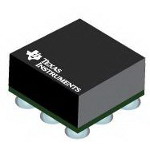
LMH2180TMX/NOPB
ActiveCLOCK FANOUT BUFFER 2-OUT 2-IN 1:1 8-PIN MICRO SMD T/R
Deep-Dive with AI
Search across all available documentation for this part.

LMH2180TMX/NOPB
ActiveCLOCK FANOUT BUFFER 2-OUT 2-IN 1:1 8-PIN MICRO SMD T/R
Technical Specifications
Parameters and characteristics for this part
| Specification | LMH2180TMX/NOPB |
|---|---|
| Differential - Input:Output | False |
| Frequency - Max [Max] | 75 MHz |
| Input | Clock |
| Mounting Type | Surface Mount |
| Number of Circuits | 1 |
| Operating Temperature [Max] | 85 °C |
| Operating Temperature [Min] | -40 °C |
| Output | Clock |
| Package / Case | 8-WFBGA |
| Ratio - Input:Output [custom] | 2:2 |
| Supplier Device Package | 8-DSBGA |
| Type | Fanout Buffer (Distribution) |
| Voltage - Supply [Max] | 5 V |
| Voltage - Supply [Min] | 2.4 V |
Pricing
Prices provided here are for design reference only. For realtime values and availability, please visit the distributors directly
| Distributor | Package | Quantity | $ | |
|---|---|---|---|---|
| Digikey | Tape & Reel (TR) | 3000 | $ 1.42 | |
| 6000 | $ 1.37 | |||
| Texas Instruments | LARGE T&R | 1 | $ 2.13 | |
| 100 | $ 1.87 | |||
| 250 | $ 1.31 | |||
| 1000 | $ 1.06 | |||
Description
General part information
LMH2180 Series
The LMH2180 is a high speed dual clock buffer designed for portable communications and applications requiring multiple accurate multi-clock systems. The LMH2180 integrates two 75 MHz low noise buffers with independent shutdown pins into a small package. The LMH2180 ensures superb system operation between the baseband and the oscillator signal path by eliminating crosstalk between the multiple clock signals.
Unique technology and design provides the LMH2180 with the ability to accurately drive both large capacitive and resistive loads. Low supply current combined with shutdown pins for each channel means the LMH2180 is ideal for battery powered applications. This part does not use an internal ground reference, thus providing additional system flexibility.
The flexible buffers provide system designers the capacity to manage complex clock signals in the latest wireless applications. Each buffer delivers 106 V/μs internal slew rate with independent shutdown and duty cycle precision. Each input is internally biased to 1V, removing the need for external resistors. Both channels have rail-to-rail inputs and outputs, a gain of one, and are AC coupled with the use of one capacitor.


