Deep-Dive with AI
Search across all available documentation for this part.

Deep-Dive with AI
Technical Specifications
Parameters and characteristics for this part
| Specification | TPS65131RGETG4 |
|---|---|
| Current - Output | 1.8 A |
| Frequency - Switching | 1.38 MHz |
| Function | Step-Up, Step-Up/Step-Down |
| Mounting Type | Surface Mount |
| Number of Outputs | 2 |
| Operating Temperature [Max] | 85 °C |
| Operating Temperature [Min] | -40 °C |
| Output Configuration | Positive and Negative (Dual Rail) |
| Output Type | Adjustable |
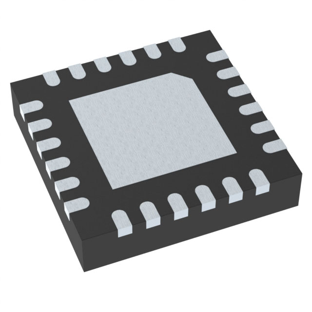
| Package / Case | 24-VFQFN Exposed Pad |
| Supplier Device Package | 24-VQFN (4x4) |
| Synchronous Rectifier | False |
| Topology | Boost, Buck-Boost |
| Voltage - Input (Max) [Max] | 5.5 V |
| Voltage - Input (Min) [Min] | 2.7 V |
| Voltage - Output (Max) | 15 V, -15 V |
| Voltage - Output (Min/Fixed) | 3.2 V |
| Voltage - Output (Min/Fixed) | -2 V |
Pricing
Prices provided here are for design reference only. For realtime values and availability, please visit the distributors directly
| Distributor | Package | Quantity | $ | |
|---|---|---|---|---|
| Digikey | Cut Tape (CT) | 1 | $ 3.38 | |
| Digi-Reel® | 1 | $ 3.38 | ||
| Tape & Reel (TR) | 250 | $ 2.36 | ||
| 500 | $ 2.12 | |||
| 1250 | $ 1.78 | |||
| 2500 | $ 1.70 | |||
Description
General part information
TPS65131-Q1 Series
The TPS65131-Q1 device is dual-output dc-dc converter generating a positive output voltage up to 15V and a negative output voltage down to –15V with output currents of typically 200mA, depending on input-voltage to output-voltage ratio. With a total efficiency up to 85%, the device is ideal for portable battery-powered equipment. The input-voltage range of 2.7V to 5.5V allows, for example, 3.3V and 5V rails to power the TPS65131-Q1 device. The TPS65131-Q1 device comes in a QFN-24 package with thermal pad and wettable flanks. Requiring few and small external components, the overall solution size can be small.
The converter operates with a fixed-frequency PWM control topology and, with power-save mode enabled, uses a pulse-skipping mode at light load currents. In operation, the typical overall device quiescent current is only 500µA. In shutdown, the device draws typically 0.2µA. Independent enable pins allow power-up and power-down sequencing for both outputs. The device has an internal current limit, overvoltage protection, and a thermal shutdown for highest reliability under fault conditions.
The TPS65131-Q1 device is qualified for automotive applications, according to AEC-Q100 temperature grade 2. The electrical characteristics are tested over –40°C to 125°C device junction temperature. This, combined with lowest shutdown currents, small solution size, package with thermal pad, plus good efficiency and protection features, targets automotive and industrial applications.
Documents
Technical documentation and resources
No documents available


