Deep-Dive with AI
Search across all available documentation for this part.

Deep-Dive with AI
Technical Specifications
Parameters and characteristics for this part
| Specification | TUSB2046BVFRG4 |
|---|---|
| Current - Supply | 40 mA |
| Function | Hub Controller |
| Interface | USB |
| Operating Temperature [Max] | 70 °C |
| Operating Temperature [Min] | 0 °C |
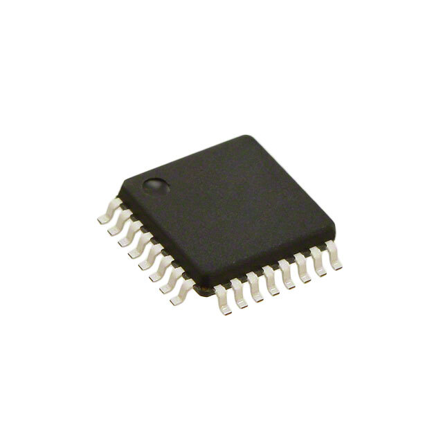
| Package / Case | 32-LQFP |
| Protocol | USB |
| Standards | USB 2.0 |
| Supplier Device Package | 32-LQFP (7x7) |
| Voltage - Supply [Max] | 3.6 V |
| Voltage - Supply [Min] | 3 V |
Pricing
Prices provided here are for design reference only. For realtime values and availability, please visit the distributors directly
| Distributor | Package | Quantity | $ | |
|---|---|---|---|---|
| Digikey | Cut Tape (CT) | 1 | $ 3.78 | |
| Digi-Reel® | 1 | $ 3.78 | ||
| N/A | 0 | $ 3.58 | ||
| Tape & Reel (TR) | 1000 | $ 2.00 | ||
| 2000 | $ 1.90 | |||
| 5000 | $ 1.83 | |||
Description
General part information
TUSB2046 Series
The TUSB2046x is a 3.3-V CMOS hub device that provides one upstream port and four downstream ports in compliance with the Universal Serial Bus (USB) specification as a full-speed hub. Because this device is implemented with a digital state machine instead of a microcontroller, no firmwareprogramming is required. Fully compliant USB transceivers are integrated into the ASIC for all upstream and downstream ports. The downstream ports support full-speed and low-speed devices by automatically setting the slew rate according to the speed of the device attached to the ports. The configuration of the BUSPWR pin selects either the bus-powered or the self-powered mode.
Configuring the GANGED input determines the power switching and overcurrent detection modes for the downstream ports. If GANGED is high, allPWRONoutputs switch together and if anyOVRCURis activated, all ports transition to the power-off state. If GANGED is low, thePWRONoutputs andOVRCURinputs operate on a per-port basis.
The TUSB2046x provides the flexibility of using a 6-MHz or a 48-MHz clock. The logic level of the TSTMODE terminal controls the selection of the clock source. When TSTMODE is low, the output of the internal APLL circuitry is selected to drive the internal core of the device. When TSTMODE is high, the TSTPLL/48MCLK input is selected as the input clock source and the APLL circuitry is powered down and bypassed. The internal oscillator cell is also powered down while TSTMODE is high. Low EMI emission is achieved because the TUSB2046x can usee a 6-MHz crystal input. Connect the crystal as shown in Figure 6. An internal PLL then generates the 48-MHz clock used to sample data from the upstream port and to synchronize the 12 MHz used for the USB clock. If low-power suspend and resume are desired, a passive crystal or resonator must be used. However, a 6-MHz oscillator may be used by connecting the output to the XTAL1 pin and leaving the XTAL2 pin open. The oscillator TTL output must not exceed 3.6 V.
Documents
Technical documentation and resources
No documents available


