8N0QV01KH-0208CDI8
ObsoleteQUAD-FREQUENCY PROGRAMMABLE VCXO
Deep-Dive with AI
Search across all available documentation for this part.

8N0QV01KH-0208CDI8
ObsoleteQUAD-FREQUENCY PROGRAMMABLE VCXO
Deep-Dive with AI
Technical Specifications
Parameters and characteristics for this part
| Specification | 8N0QV01KH-0208CDI8 |
|---|---|
| null | |
Pricing
Prices provided here are for design reference only. For realtime values and availability, please visit the distributors directly
| Distributor | Package | Quantity | $ | |
|---|---|---|---|---|
Description
General part information
8N0QV01 Series
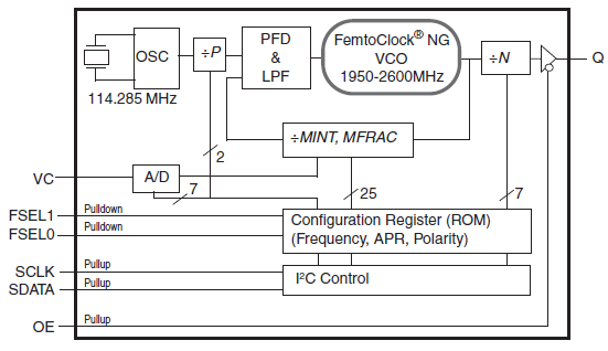
The 8N0QV01 is a Quad-Frequency Programmable VCXO with very flexible frequency and pull-range programming capabilities. The device uses IDT’s Fourth Generation FemtoClock® NG technology for an optimum of high clock frequency and low phase noise performance. The device accepts 2.5V or 3.3V supply and ispackaged in a small, lead-free (RoHS 6) 10-lead ceramic 5mm x 7mm x 1.55mm package.Besides the four default power-up frequencies set by the FSEL0 and FSEL1 pins, the 8N0QV01 can be programmed via the I2C interface to any output clock frequency between 15.476MHz to 260MHz to a very high degree of precision with a frequency step size of 435.9Hz ÷N (N: PLL post divider). Since the FSEL0 and FSEL1 pins are mapped to four independent PLL, P, M and N divider registers (P, MINT, MFRAC and N), reprogramming those registers to other frequencies under control of FSEL0 and FSEL1 is supported. The extended temperature range supports wireless infrastructure, telecommunication and networking end equipment requirements.
Documents
Technical documentation and resources
No documents available


