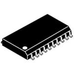
MC100LVEL91DWR2
ActiveTRANSLATOR LVPECL TO ECL 3-CH UNIDIRECTIONAL 20-PIN SOIC W T/R
Deep-Dive with AI
Search across all available documentation for this part.

MC100LVEL91DWR2
ActiveTRANSLATOR LVPECL TO ECL 3-CH UNIDIRECTIONAL 20-PIN SOIC W T/R
Deep-Dive with AI
Technical Specifications
Parameters and characteristics for this part
| Specification | MC100LVEL91DWR2 |
|---|---|
| Channel Type | Unidirectional |
| Channels per Circuit | 3 |
| Input Signal | LVPECL |
| Mounting Type | Surface Mount |
| Number of Circuits | 1 |
| Operating Temperature [Max] | 85 °C |
| Operating Temperature [Min] | -40 °C |
| Output Signal | ECL |
| Output Type | Differential |
| Package / Case | 20-SOIC |
| Package / Case [y] | 0.295 in |
| Package / Case [y] | 7.5 mm |
| Supplier Device Package | 20-SOIC |
| Translator Type | Mixed Signal |
Pricing
Prices provided here are for design reference only. For realtime values and availability, please visit the distributors directly
| Distributor | Package | Quantity | $ | |
|---|---|---|---|---|
| Digikey | Bulk | 93 | $ 3.26 | |
Description
General part information
MC100LVEL91 Series
The MC100LVEL91 is a triple LVPECL input to ECL output translator. The device receives standard or low voltage differential PECL signals, determined by the VCC supply level, and translates them to differential -3.3 V to -5.0 V ECL output signals. (For translation from 5.0 V PECL to -5 V ECL output, see MC100EL91.)To accomplish the level translation the LVEL91 requires three power rails. The VCCsupply should be connected to the positive supply, and the VEEpin should be connected to the negative power supply. The GND pins are connected to the system ground plane. Both VEEand VCCshould be bypassed to ground via 0.01 µF capacitors.Under open input conditions, the Dbar input will be biased at VCC/2 and the D input will be pulled to GND. This condition will force the Q output to a low, ensuring stability.The VBBpin, an internally generated voltage supply, is available to this device only. For single-ended input conditions, the unused differential input is connected to VBBas a switching reference voltage. VBBmay also rebias AC coupled inputs. When used, decouple VBBand VCCvia a 0.01 µF capacitor and limit current sourcing or sinking to 0.5 mA. When not used, VBBshould be left open.
Documents
Technical documentation and resources


