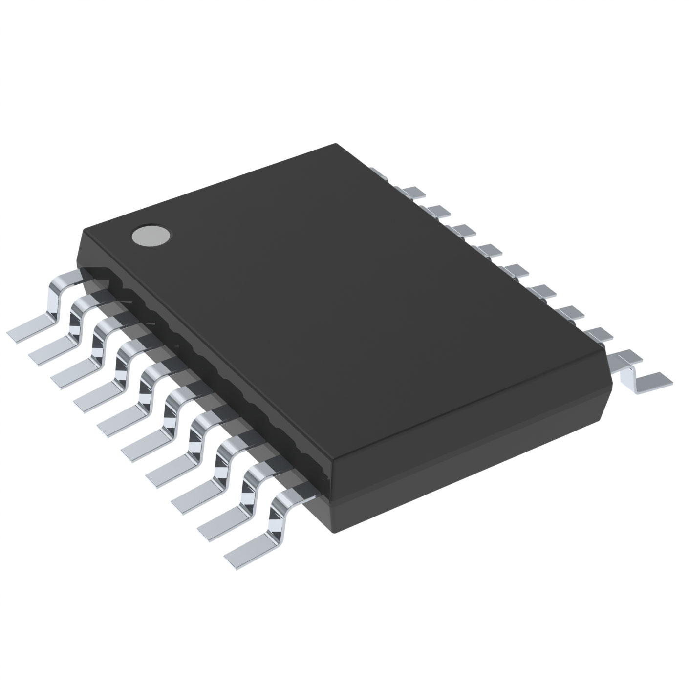
SN74AS885DWR
ObsoleteMAGNITUDE COMPARATOR 8-BIT 24-PIN SOIC T/R
Deep-Dive with AI
Search across all available documentation for this part.

SN74AS885DWR
ObsoleteMAGNITUDE COMPARATOR 8-BIT 24-PIN SOIC T/R
Deep-Dive with AI
Technical Specifications
Parameters and characteristics for this part
| Specification | SN74AS885DWR |
|---|---|
| Current - Output High, Low [custom] | 20 mA |
| Current - Output High, Low [custom] | 2 mA |
| Max Propagation Delay @ V, Max CL | 17.5 ns |
| Mounting Type | Surface Mount |
| Number of Bits | 8 |
| Operating Temperature [Max] | 70 °C |
| Operating Temperature [Min] | 0 °C |
| Output | Active High |
| Output Function | A>B, A<B |
| Package / Case | 24-SOIC |
| Package / Case [custom] | 7.5 mm |
| Package / Case [custom] | 0.295 in |
| Supplier Device Package | 24-SOIC |
| Type | Magnitude Comparator |
| Voltage - Supply [Max] | 5.5 V |
| Voltage - Supply [Min] | 4.5 V |
Pricing
Prices provided here are for design reference only. For realtime values and availability, please visit the distributors directly
| Distributor | Package | Quantity | $ | |
|---|---|---|---|---|
Description
General part information
SN74AS885 Series
These advanced Schottky devices are capable of performing high-speed arithmetic or logic comparisons on two 8-bit binary or two's complement words. Two fully decoded decisions about words P and Q are externally available at two outputs. These devices are fully expandable to any number of bits without external gates. To compare words of longer lengths, the P > QOUT and P < QOUT outputs of a stage handling less significant bits can be connected to the P > QIN and P < QIN inputs of the next stage handling more significant bits. The cascading paths are implemented with only a two-gate-level delay to reduce overall comparison times for long words. Two alternative methods of cascading are shown in application information.
The latch is transparent when P latch-enable (PLE) input is high; the P-input port is latched
when PLE is low. This provides the designer with temporary storage for the P-data word. The enable circuitry is implemented with minimal delay times to enhance performance when cascaded for longer words. The PLE, P, and Q data inputs utilize pnp input transistors to reduce the low-level current input requirement to typically -0.25 mA, which minimizes dc loading effects.
Documents
Technical documentation and resources


