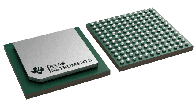
ADC12DJ5200RFAAVT
ActiveRF-SAMPLING 12-BIT ADC WITH DUAL-CHANNEL 5.2 GSPS OR SINGLE-CHANNEL 10.4 GSPS
Deep-Dive with AI
Search across all available documentation for this part.

ADC12DJ5200RFAAVT
ActiveRF-SAMPLING 12-BIT ADC WITH DUAL-CHANNEL 5.2 GSPS OR SINGLE-CHANNEL 10.4 GSPS
Technical Specifications
Parameters and characteristics for this part
| Specification | ADC12DJ5200RFAAVT |
|---|---|
| Architecture | Pipelined, SAR |
| Configuration | MUX-ADC |
| Data Interface | JESD204B/C |
| Features | Temperature Sensor |
| Input Type | Single Ended, Differential |
| Mounting Type | Surface Mount |
| Number of A/D Converters | 2 |
| Number of Bits | 12 bits |
| Number of Inputs | 2 |
| Operating Temperature [Max] | 85 °C |
| Operating Temperature [Min] | -40 °C |
| Package / Case | FCBGA, 144-FBGA |
| Ratio - S/H:ADC | 0:2 |
| Reference Type | External, Internal |
| Sampling Rate (Per Second) | 5.2 G |
| Supplier Device Package | 144-FCBGA (10x10) |
| Voltage - Supply, Analog [Max] | 2 V, 1.15 V |
| Voltage - Supply, Analog [Min] | 1.8 V, 1.05 V |
| Voltage - Supply, Digital [Max] | 1.15 V |
| Voltage - Supply, Digital [Min] | 1.05 V |
Pricing
Prices provided here are for design reference only. For realtime values and availability, please visit the distributors directly
| Distributor | Package | Quantity | $ | |
|---|---|---|---|---|
| Digikey | Tape & Reel (TR) | 250 | $ 2847.50 | |
| Texas Instruments | SMALL T&R | 1 | $ 2733.60 | |
| 100 | $ 2505.80 | |||
| 250 | $ 2369.12 | |||
| 1000 | $ 2278.00 | |||
Description
General part information
ADC12DJ5200RF Series
The ADC12DJ5200RF device is an RF-sampling, giga-sample, analog-to-digital converter (ADC) that can directly sample input frequencies from DC to above 10GHz. ADC12DJ5200RF can be configured as a dual-channel, 5.2GSPS ADC or single-channel, 10.4GSPS ADC. Support of a useable input frequency range of up to 10GHz enables direct RF sampling of L-band, S-band, C-band, and X-band for frequency agile systems.
The ADC12DJ5200RF uses a high-speed JESD204C output interface with up to 16 serialized lanes supporting up to 17.16Gbps line rate. Deterministic latency and multi-device synchronization is supported through JESD204C subclass-1. The JESD204C interface can be configured to trade-off line rate and number of lanes. Both 8b/10b and 64b/66b data encoding schemes are supported. 64b/66b encoding supports forward error correction (FEC) for improved bit error rates. The interface is backwards compatible with JESD204B receivers.
Innovative synchronization features, including noiseless aperture delay adjustment and SYSREF windowing, simplify system design for multi-channel applications. Optional digital down converters (DDCs) are available to provide digital conversion to baseband and to reduce the interface rate. A programmable FIR filter allows on-chip equalization.
Documents
Technical documentation and resources


