Deep-Dive with AI
Search across all available documentation for this part.

Deep-Dive with AI
Technical Specifications
Parameters and characteristics for this part
| Specification | TMS5701115BZWTQQ1 |
|---|---|
| Connectivity | SPI, FlexRay, SCI, I2C, UART/USART, EBI/EMI, LINbus, MibSPI, CANbus |
| Core Processor | ARM® Cortex®-R4F |
| Core Size [Max] | 32 Bit |
| Core Size [Min] | 16 Bit |
| Data Converters [custom] | 12 |
| Data Converters [custom] | 24 |
| EEPROM Size | 64 K |
| Grade | Automotive |
| Mounting Type | Surface Mount |
| Number of I/O | 101 |
| Operating Temperature [Max] | 125 °C |
| Operating Temperature [Min] | -40 °C |
| Oscillator Type | External |
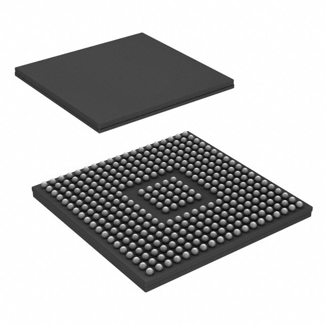
| Package / Case | 337-LFBGA |
| Peripherals | WDT, DMA, PWM, POR |
| Program Memory Size | 1 MB |
| Program Memory Type | FLASH |
| Qualification | AEC-Q100 |
| RAM Size | 128 K |
| Speed | 180 MHz |
| Supplier Device Package | 337-NFBGA (16x16) |
| Voltage - Supply (Vcc/Vdd) [Max] | 3.6 V |
| Voltage - Supply (Vcc/Vdd) [Min] | 1.14 V |
Pricing
Prices provided here are for design reference only. For realtime values and availability, please visit the distributors directly
| Distributor | Package | Quantity | $ | |
|---|---|---|---|---|
Description
General part information
TMS570LS1224 Series
The TMS570LS1227 device is a high-performance automotive-grade microcontroller family for safety systems. The safety architecture includes dual CPUs in lockstep, CPU and memory BIST logic, ECC on both the flash and the data SRAM, parity on peripheral memories, and loopback capability on peripheral I/Os.
The TMS570LS1227 device integrates the ARM Cortex-R4F floating-point CPU which offers an efficient 1.66 DMIPS/MHz, and has configurations which can run up to 180 MHz providing up to 298 DMIPS. The device supports the word-invariant big-endian [BE32] format.
The TMS570LS1227 device has 1.25MB of integrated flash and 192KB of data RAM with single-bit error correction and double-bit error detection. The flash memory on this device is a nonvolatile, electrically erasable and programmable memory, implemented with a 64-bit-wide data bus interface. The flash operates on a 3.3-V supply input (same level as I/O supply) for all read, program, and erase operations. When in pipeline mode, the flash operates with a system clock frequency of up to 180 MHz. The SRAM supports single-cycle read and write accesses in byte, halfword, word, and double-word modes throughout the supported frequency range.
Documents
Technical documentation and resources
No documents available


