Deep-Dive with AI
Search across all available documentation for this part.

Deep-Dive with AI
Technical Specifications
Parameters and characteristics for this part
| Specification | 74GTLPH306DGVR |
|---|---|
| Channel Type | Bidirectional |
| Channels per Circuit | 8 |
| Input Signal | LVTTL |
| Mounting Type | Surface Mount |
| Number of Circuits | 1 |
| Operating Temperature [Max] | 85 °C |
| Operating Temperature [Min] | -40 °C |
| Output Signal | GTLP |
| Output Type | Tri-State, Non-Inverted |
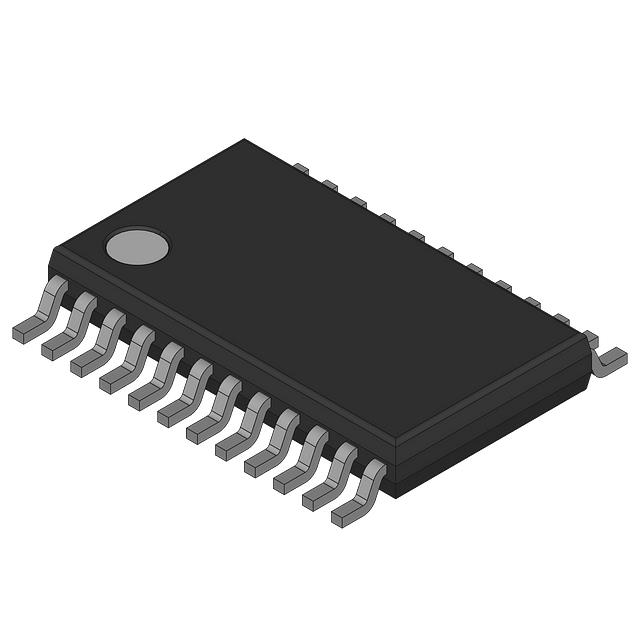
| Package / Case | 24-TFSOP |
| Package / Case [y] | 4.4 mm |
| Package / Case [y] | 0.173 in |
| Supplier Device Package | 24-TVSOP |
| Translator Type | Mixed Signal |
Pricing
Prices provided here are for design reference only. For realtime values and availability, please visit the distributors directly
| Distributor | Package | Quantity | $ | |
|---|---|---|---|---|
| Digikey | Bulk | 81 | $ 3.72 | |
Description
General part information
SN74GTLPH306 Series
The SN74GTLPH306 is a medium-drive, 8-bit bus transceiver that provides LVTTL-to-GTLP and GTLP-to-LVTTL signal-level translation. The device provides a high-speed interface between cards operating at LVTTL logic levels and a backplane operating at GTLP signal levels. High-speed (about three times faster than standard LVTTL or TTL) backplane operation is a direct result of GTLP's reduced output swing (<1 V), reduced input threshold levels, improved differential input, OEC™ circuitry, and TI-OPC™ circuitry. Improved GTLP OEC and TI-OPC circuits minimize bus-settling time and have been designed and tested using several backplane models. The medium drive allows incident-wave switching in heavily loaded backplanes with equivalent load impedance down to 19.
GTLP is the Texas Instruments (TI™) derivative of the Gunning Transceiver Logic (GTL) JEDEC standard JESD 8-3. The ac specification of the SN74GTLPH306 is given only at the preferred higher-noise-margin GTLP, but the user has the flexibility of using this device at either GTL (VTT= 1.2 V and VREF= 0.8 V) or GTLP (VTT= 1.5 V and VREF= 1 V) signal levels.
Normally, the B port operates at GTLP signal levels. The A-port and control inputs operate at LVTTL logic levels, but are 5-V tolerant and are compatible with TTL and 5-V CMOS inputs. VREFis the B-port differential input reference voltage.
Documents
Technical documentation and resources


