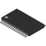
THS1009IDA
Active10-BIT, 8 MSPS ADC DUAL CH., PARALLEL DSP/UP, CHANNEL AUTOSCAN, LOW POWER
Deep-Dive with AI
Search across all available documentation for this part.

THS1009IDA
Active10-BIT, 8 MSPS ADC DUAL CH., PARALLEL DSP/UP, CHANNEL AUTOSCAN, LOW POWER
Deep-Dive with AI
Technical Specifications
Parameters and characteristics for this part
| Specification | THS1009IDA |
|---|---|
| Architecture | Pipelined |
| Configuration | S/H-MUX-ADC |
| Data Interface | Parallel |
| Features | Simultaneous Sampling |
| Input Type | Single Ended, Differential |
| Mounting Type | Surface Mount |
| Number of A/D Converters | 1 |
| Number of Bits [custom] | 10 |
| Number of Inputs | 1, 2 |
| Operating Temperature [Max] | 85 °C |
| Operating Temperature [Min] | -40 °C |
| Package / Case | 32-TSSOP |
| Ratio - S/H:ADC | |
| Reference Type | External, Internal |
| Sampling Rate (Per Second) | 8 M |
| Supplier Device Package | 32-TSSOP |
| Voltage - Supply, Analog | 5 V |
| Voltage - Supply, Digital | 5 V |
Pricing
Prices provided here are for design reference only. For realtime values and availability, please visit the distributors directly
| Distributor | Package | Quantity | $ | |
|---|---|---|---|---|
| Digikey | Tube | 92 | $ 13.77 | |
| Texas Instruments | TUBE | 1 | $ 13.89 | |
| 100 | $ 12.13 | |||
| 250 | $ 9.35 | |||
| 1000 | $ 8.37 | |||
Description
General part information
THS1009 Series
The THS1009 is a CMOS, low-power, 10-bit, 8 MSPS analog-to-digital converter (ADC). The speed, resolution, bandwidth, and single-supply operation are suited for applications in radar, imaging, high-speed acquisition, and communications. A multistage pipelined architecture with output error correction logic provides for no missing codes over the full operating temperature range. Internal control registers allow for programming the ADC into the desired mode. The THS1009 consists of two analog inputs, which are sampled simultaneously. These inputs can be selected individually and configured to single-ended or differential inputs. Internal reference voltages for the ADC (1.5 V and 3.5 V) are provided. An external reference can also be chosen to suit the dc accuracy and temperature drift requirements of the application.
The THS1009C is characterized for operation from 0°C to 70°C, and the THS1009I is characterized for operation from –40°C to 85°C.
The THS1009 is a CMOS, low-power, 10-bit, 8 MSPS analog-to-digital converter (ADC). The speed, resolution, bandwidth, and single-supply operation are suited for applications in radar, imaging, high-speed acquisition, and communications. A multistage pipelined architecture with output error correction logic provides for no missing codes over the full operating temperature range. Internal control registers allow for programming the ADC into the desired mode. The THS1009 consists of two analog inputs, which are sampled simultaneously. These inputs can be selected individually and configured to single-ended or differential inputs. Internal reference voltages for the ADC (1.5 V and 3.5 V) are provided. An external reference can also be chosen to suit the dc accuracy and temperature drift requirements of the application.
Documents
Technical documentation and resources


