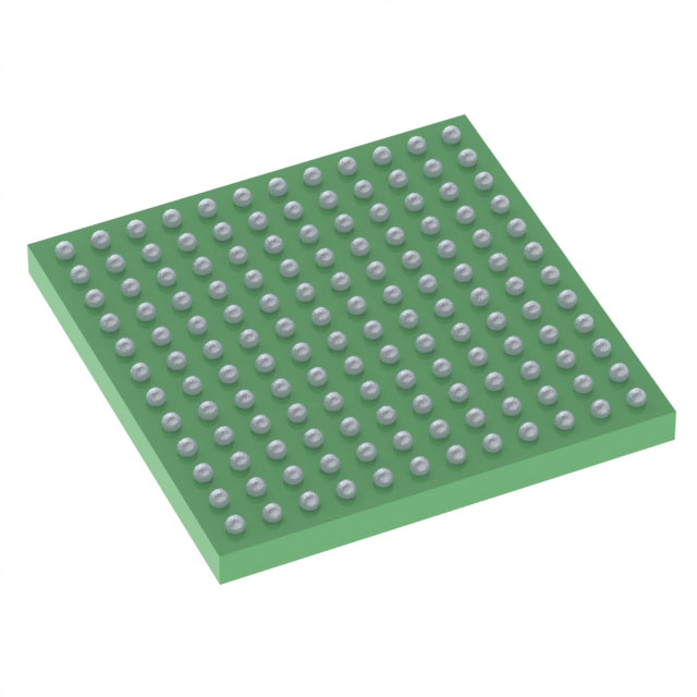
ADC12QJ800AAVQ1
ActiveAUTOMOTIVE QUAD-CHANNEL, 12-BIT, 800-MSPS ANALOG-TO-DIGITAL CONVERTER (ADC) WITH JESD204C INTERFACE
Deep-Dive with AI
Search across all available documentation for this part.

ADC12QJ800AAVQ1
ActiveAUTOMOTIVE QUAD-CHANNEL, 12-BIT, 800-MSPS ANALOG-TO-DIGITAL CONVERTER (ADC) WITH JESD204C INTERFACE
Technical Specifications
Parameters and characteristics for this part
| Specification | ADC12QJ800AAVQ1 |
|---|---|
| Architecture | SAR |
| Configuration | ADC |
| Data Interface | JESD204B Serial |
| Input Type | Differential |
| Mounting Type | Surface Mount |
| Number of A/D Converters | 4 |
| Number of Bits | 12 bits |
| Number of Inputs | 8 |
| Operating Temperature [Max] | 125 °C |
| Operating Temperature [Min] | -40 °C |
| Package / Case | FCBGA, 144-FBGA |
| Ratio - S/H:ADC | 0:4 |
| Reference Type | External |
| Sampling Rate (Per Second) | 800 M |
| Supplier Device Package | 144-FCBGA (10x10) |
| Voltage - Supply, Analog [Max] | 2 V, 1.15 V |
| Voltage - Supply, Analog [Min] | 1.8 V, 1.05 V |
| Voltage - Supply, Digital [Max] | 1.15 V |
| Voltage - Supply, Digital [Min] | 1.05 V |
Pricing
Prices provided here are for design reference only. For realtime values and availability, please visit the distributors directly
| Distributor | Package | Quantity | $ | |
|---|---|---|---|---|
| Digikey | Tray | 4 | $ 216.13 | |
| 12 | $ 207.00 | |||
| 28 | $ 202.44 | |||
| Texas Instruments | JEDEC TRAY (5+1) | 1 | $ 174.81 | |
| 100 | $ 158.24 | |||
| 250 | $ 153.71 | |||
| 1000 | $ 150.70 | |||
Description
General part information
ADC12QJ800-Q1 Series
ADC12xJ800-Q1 is a family of quad, dual and single channel, 12-bit, 800MSPS analog-to-digital converters (ADC). Low power consumption, high sampling rate and 12-bit resolution makes the ADC12xJ800-Q1 suited for light detection and ranging (LiDAR) systems. The ADC12xJ800-Q1 is qualified for automotive applications.
Full-power input bandwidth (-3dB) of 6GHz provides flat frequency response for frequency modulated continuous wave (FMCW) LiDAR systems and provides a narrow impulse response for pulse-based systems. The full-power input bandwidth also enables direct RF sampling of L-band and S-band.
A number of clocking features are included to relax system hardware requirements, such as an internal phase-locked loop (PLL) with integrated voltage-controlled oscillator (VCO) to generate the sampling clock. Four clock outputs are provided to clock the logic and SerDes of the FPGA or ASIC. A timestamp input and output is provided for pulsed systems.
Documents
Technical documentation and resources


