Deep-Dive with AI
Search across all available documentation for this part.

Deep-Dive with AI
Technical Specifications
Parameters and characteristics for this part
| Specification | 74VHC273MTC |
|---|---|
| Clock Frequency | 110 MHz |
| Current - Output High, Low [custom] | 8 mA |
| Current - Output High, Low [custom] | 8 mA |
| Current - Quiescent (Iq) | 4 çA |
| Input Capacitance | 4 pF |
| Max Propagation Delay @ V, Max CL | 11 ns |
| Mounting Type | Surface Mount |
| Number of Bits per Element | 8 |
| Number of Elements | 1 |
| Operating Temperature [Max] | 85 °C |
| Operating Temperature [Min] | -40 °C |
| Output Type | Non-Inverted |
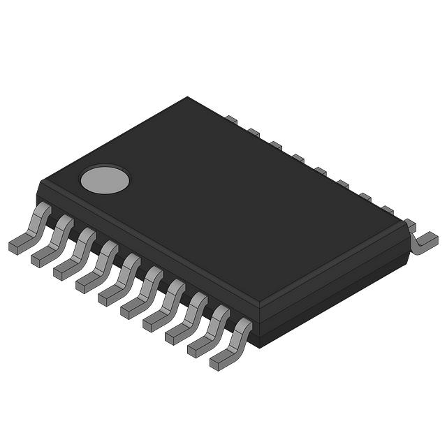
| Package / Case | 20-TSSOP |
| Package / Case [x] | 0.173 in |
| Package / Case [y] | 4.4 mm |
| Supplier Device Package | 20-TSSOP |
| Trigger Type | Positive Edge |
| Type | D-Type |
| Voltage - Supply [Max] | 5.5 V |
| Voltage - Supply [Min] | 2 V |
Pricing
Prices provided here are for design reference only. For realtime values and availability, please visit the distributors directly
| Distributor | Package | Quantity | $ | |
|---|---|---|---|---|
| Digikey | Bulk | 876 | $ 0.34 | |
| 876 | $ 0.34 | |||
Description
General part information
74VHC273 Series
The VHC273 is an advanced high speed CMOS Octal D-type flip-flop fabricated with silicon gate CMOS technology. It achieves the high speed operation similar to equivalent Bipolar Schottky TTL while maintaining the CMOS low power dissipation. The register has a common buffered Clock (CP) which is fully edge-triggered. The state of each D input, one setup time before the LOW-to-HIGH clock transition, is transferred to the corresponding flip-flop's Q output. The Master Reset (MR#) input will clear all flip-flops simultaneously. All outputs will be forced LOW independently of Clock or Data inputs by a LOW voltage level on the MR# input. An input protection circuit insures that 0V to 7V can be applied to the inputs pins without regard to the supply voltage. This device can be used to interface 5V to 3V systems and two supply systems such as battery backup. This circuit prevents device destruction due to mismatched supply and input voltages.
Documents
Technical documentation and resources


