Deep-Dive with AI
Search across all available documentation for this part.

Deep-Dive with AI
Technical Specifications
Parameters and characteristics for this part
| Specification | TPS61041DBVRG4 |
|---|---|
| Applications | Backlight |
| Current - Output / Channel | 215 mA |
| Dimming | PWM |
| Frequency | 1 MHz |
| Internal Switch(s) | True |
| Mounting Type | Surface Mount |
| Number of Outputs | 1 |
| Operating Temperature [Max] | 85 C |
| Operating Temperature [Min] | -40 ¯C |
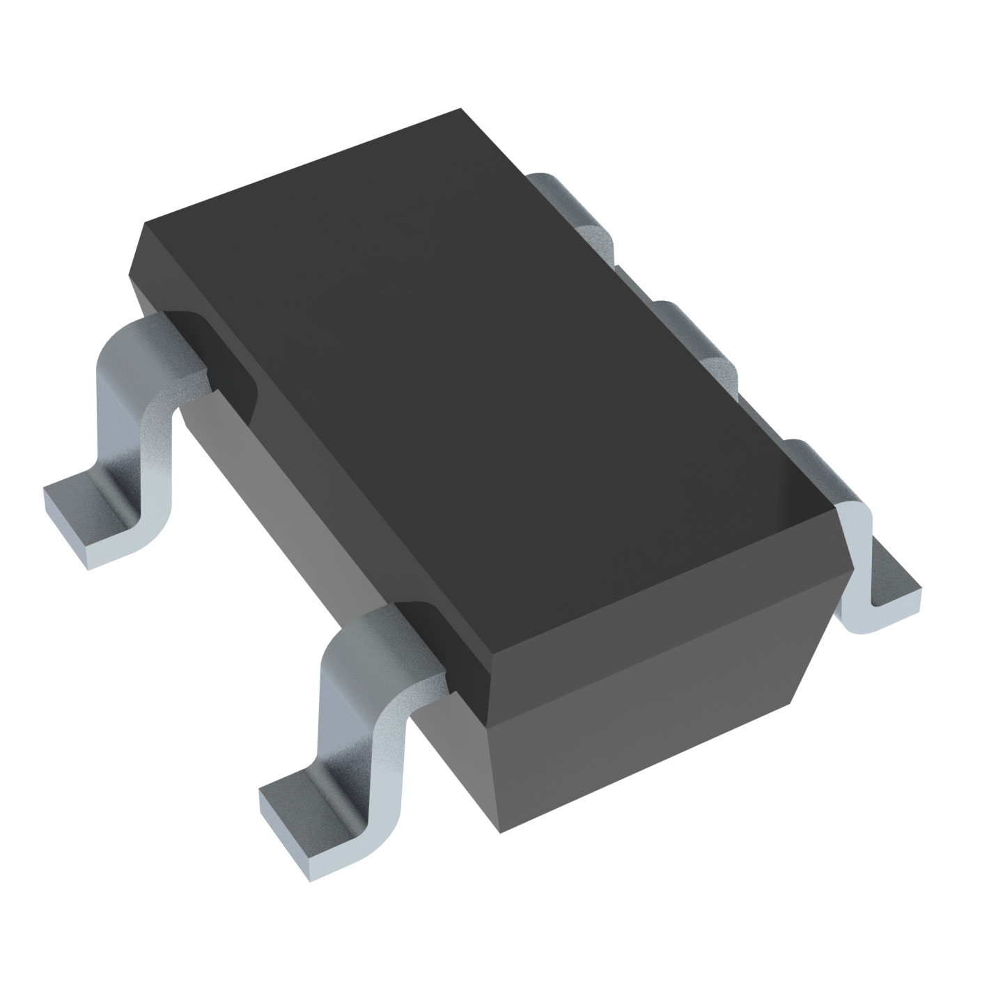
| Package / Case | SOT-753, SC-74A |
| Supplier Device Package | SOT-23-5 |
| Topology | Step-Up (Boost) |
| Type | DC DC Regulator |
| Voltage - Output | 28 V |
| Voltage - Supply (Max) [Max] | 6 V |
| Voltage - Supply (Min) [Min] | 1.8 V |
Pricing
Prices provided here are for design reference only. For realtime values and availability, please visit the distributors directly
| Distributor | Package | Quantity | $ | |
|---|---|---|---|---|
| Digikey | N/A | 3000 | $ 0.67 | |
| Tape & Reel (TR) | 3000 | $ 0.68 | ||
| 6000 | $ 0.65 | |||
| 15000 | $ 0.63 | |||
Description
General part information
TPS61041 Series
The TPS6104x is a high-frequency boost converter dedicated for small to medium LCD bias supply and white LED backlight supplies. The device is ideal to generate output voltages up to 28 V from a dual-cell NiMH/NiCd or a single-cell Li-Ion battery. The part can also be used to generate standard 3.3-V or 5-V to 12-V power conversions.
The TPS6104x operates with a switching frequency up to 1 MHz. This frequency allows the use of small external components using ceramic as well as tantalum output capacitors. Together with the thin WSON package, the TPS6104x gives a very small overall solution size. The TPS61040 device has an internal 400-mA switch current limit, while the TPS61041 device has a 250-mA switch current limit, offering lower output voltage ripple and allows the use of a smaller form factor inductor for lower power applications. The low quiescent current (typically 28 µA) together with an optimized control scheme, allows device operation at very high efficiencies over the entire load current range.
The TPS6104x is a high-frequency boost converter dedicated for small to medium LCD bias supply and white LED backlight supplies. The device is ideal to generate output voltages up to 28 V from a dual-cell NiMH/NiCd or a single-cell Li-Ion battery. The part can also be used to generate standard 3.3-V or 5-V to 12-V power conversions.
Documents
Technical documentation and resources
No documents available


