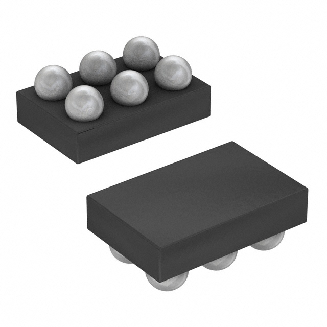
MAX8531EBTGGJ+T
ObsoleteIC REG LINEAR 3V/3V 6UCSP
Deep-Dive with AI
Search across all available documentation for this part.

MAX8531EBTGGJ+T
ObsoleteIC REG LINEAR 3V/3V 6UCSP
Deep-Dive with AI
Technical Specifications
Parameters and characteristics for this part
| Specification | MAX8531EBTGGJ+T |
|---|---|
| Control Features | Enable, Reset |
| Current - Output | 150 mA, 0.2 A |
| Current - Quiescent (Iq) | 220 µA |
| Mounting Type | Surface Mount |
| Number of Regulators | 2 |
| Operating Temperature [Max] | 85 C |
| Operating Temperature [Min] | -40 ¯C |
| Output Configuration | Positive |
| Package / Case | WLBGA, 6-WFBGA |
| Protection Features | Over Temperature, Over Current, Short Circuit |
| PSRR | 62 dB |
| Supplier Device Package | 6-WLP |
| Voltage - Input (Max) [Max] | 6.5 V |
| Voltage - Output (Min/Fixed) [Max] | 3 V |
| Voltage - Output (Min/Fixed) [Min] | 3 V |
Pricing
Prices provided here are for design reference only. For realtime values and availability, please visit the distributors directly
| Distributor | Package | Quantity | $ | |
|---|---|---|---|---|
| Digikey | N/A | 0 | $ 1.06 | |
Description
General part information
MAX8531 Series
The MAX8530/MAX8531 offer the benefits of low-dropout voltage and ultra-low power regulation in subminiaturized UCSP and QFN packages with an integrated microprocessor reset circuit (MAX8530 only). The devices operate from a 2.5V to 6.5V input and deliver up to 200mA and 150mA outputs with low dropout of 100mV (typ) at 100mA. Designed with an internal P-channel MOSFET pass transistor, the supply current is kept at a low 130µA (with both LDOs on), independent of the load current and dropout voltage. Other features include short-circuit protection and thermal-shutdown protection.The MAX8530 provides microprocessor open-drain, active-low reset output to monitor OUT1, eliminating external components and adjustments. The MAX8530 asserts a 100ms (min) RESET-bar signal when OUT1 drops below 87% of the nominal output voltage. The MAX8531 includes a reference bypass pin for low output noise (40µVRMS).Both devices include a logic-controlled shutdown input and are available in 6-bump UCSP and 6-pin thin QFN exposed pad packages.ApplicationsCell Phones/Cordless PhonesDigital CamerasHandheld Instruments (PDAs, Palmtops)Notebook ComputersPCMCIA CardsPDAs and Palmtop ComputersWireless Local Area Networks (WLANs)
Documents
Technical documentation and resources
No documents available


