Zenode.ai Logo
Beta
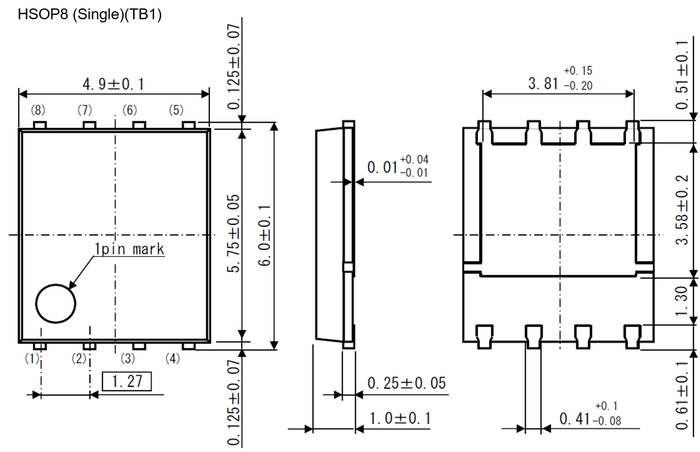
Product dimension image
Discrete Semiconductor Products

RS6G122CHTB1

Active
Rohm Semiconductor

NCH 40V 225A, HSOP8, POWER MOSFET

Deep-Dive with AI

Search across all available documentation for this part.

Product dimension image
Discrete Semiconductor Products

RS6G122CHTB1

Active
Rohm Semiconductor

NCH 40V 225A, HSOP8, POWER MOSFET

Technical Specifications

Parameters and characteristics for this part

SpecificationRS6G122CHTB1
Current - Continuous Drain (Id) @ 25°C225 A, 120 A
Drain to Source Voltage (Vdss)40 V
Drive Voltage (Max Rds On, Min Rds On)10 V, 6 V
FET TypeN-Channel
Gate Charge (Qg) (Max) @ Vgs [Max]52 nC
Input Capacitance (Ciss) (Max) @ Vds [Max]3800 pF
Mounting TypeSurface Mount
Operating Temperature175 °C
Package / Case8-PowerTDFN
Power Dissipation (Max)3.6 W, 125 W
Rds On (Max) @ Id, Vgs1.2 mOhm
Supplier Device Package8-HSOP
TechnologyMOSFET (Metal Oxide)
Vgs (Max)20 V

Pricing

Prices provided here are for design reference only. For realtime values and availability, please visit the distributors directly

DistributorPackageQuantity$
DigikeyN/A 2500$ 3.03

Description

General part information

RS6G122CH Series

RS6G122CH is a power MOSFET with low on-resistance and high power package, suitable for switching, motor drives, and DC/DC converter.

Documents

Technical documentation and resources

How to Use LTspice® Models

Schematic Design & Verification

HSOP8(TB1) Taping Information

Package Information

About Flammability of Materials

Environmental Data

Part Explanation

Application Note

Impedance Characteristics of Bypass Capacitor

Schematic Design & Verification

Compliance of the RoHS directive

Environmental Data

Calculation of Power Dissipation in Switching Circuit

Schematic Design & Verification

Condition of Soldering / Land Pattern Reference

Package Information

RS6G122CH Data Sheet

Data Sheet

Importance of Probe Calibration When Measuring Power: Deskew

Schematic Design & Verification

Notes for Temperature Measurement Using Thermocouples

Thermal Design

Temperature derating method for Safe Operating Area (SOA)

Schematic Design & Verification

Types and Features of Transistors

Application Note

What is a Thermal Model? (Transistor)

Thermal Design

Moisture Sensitivity Level - Transistors

Package Information

Two-Resistor Model for Thermal Simulation

Thermal Design

How to Use LTspice® Models: Tips for Improving Convergence

Schematic Design & Verification

Method for Calculating Junction Temperature from Transient Thermal Resistance Data

Thermal Design

About Export Regulations

Export Information

List of Transistor Package Thermal Resistance

Thermal Design

Notes for Calculating Power Consumption:Static Operation

Thermal Design

Notes for Temperature Measurement Using Forward Voltage of PN Junction

Thermal Design

Method for Monitoring Switching Waveform

Schematic Design & Verification

Measurement Method and Usage of Thermal Resistance RthJC

Thermal Design

MOSFET Gate Drive Current Setting for Motor Driving

Technical Article

Taping Information

Package Information

Anti-Whisker formation - Transistors

Package Information

PCB Layout Thermal Design Guide

Thermal Design

Precautions When Measuring the Rear of the Package with a Thermocouple

Thermal Design

HSOP8(TB1) Dimension

Package Information

HSOP8(TB1) Explanation for Marking

Package Information

What Is Thermal Design

Thermal Design

MOSFET Gate Resistor Setting for Motor Driving

Technical Article

Basics of Thermal Resistance and Heat Dissipation

Thermal Design

Overview of ROHM's Simulation Models(for ICs and Discrete Semiconductors)

Technical Article