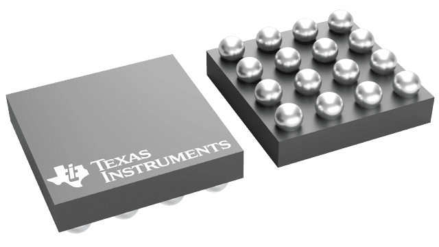
LM3279TLX/NOPB
ActiveBUCK-BOOST CONVERTER WITH MIPI® RFFE INTERFACE FOR 3G AND 4G RF POWER AMPLIFIERS
Deep-Dive with AI
Search across all available documentation for this part.

LM3279TLX/NOPB
ActiveBUCK-BOOST CONVERTER WITH MIPI® RFFE INTERFACE FOR 3G AND 4G RF POWER AMPLIFIERS
Technical Specifications
Parameters and characteristics for this part
| Specification | LM3279TLX/NOPB |
|---|---|
| Applications | 3.5G, Converter, 4G RF Power Amplifier, 3G |
| Mounting Type | Surface Mount |
| Number of Outputs | 1 |
| Operating Temperature [Max] | 85 °C |
| Operating Temperature [Min] | -30 ░C |
| Package / Case | 16-WFBGA, DSBGA |
| Supplier Device Package | 16-DSBGA (2.5x2.12) |
| Voltage - Input [Max] | 5.5 V |
| Voltage - Input [Min] | 2.7 V |
| Voltage - Output [Max] | 4.2 V |
| Voltage - Output [Min] | 0.4 V |
Pricing
Prices provided here are for design reference only. For realtime values and availability, please visit the distributors directly
| Distributor | Package | Quantity | $ | |
|---|---|---|---|---|
| Digikey | Tape & Reel (TR) | 3000 | $ 1.13 | |
| 6000 | $ 1.08 | |||
| Texas Instruments | LARGE T&R | 1 | $ 1.85 | |
| 100 | $ 1.53 | |||
| 250 | $ 1.10 | |||
| 1000 | $ 0.83 | |||
Description
General part information
LM3279 Series
The LM3279 is a buck-boost DC/DC converter designed to generate output voltages above or below a given input voltage and is particularly suitable for Power Amplifiers operating from single-cell Li-Ion batteries in portable applications.
The LM3279 has four modes of operation: Pulse Width Modulation (PWM), Pulse Frequency Modulation (PFM), standby, and shutdown. During normal conditions, the LM3279 operates in full synchronous PWM mode at 2.4-MHz typical switching frequency, providing seamless transitions between buck and boost operating regimes. Energy-saving PFM mode increases efficiencies and current savings during low-power RF transmission modes. For high-transmit power, the device operates in PWM buck or boost mode, whereas the device can transition between PWM and PFM modes during low-power transmit. The LM3279 can be controlled either via an included MIPI RFFE Digital Control Interface or by using an analog control from an external MCU, offering design flexibility.
The power converter topology enables minimum total solution size by using one small footprint and case size inductor and two surface mount capacitors.
Documents
Technical documentation and resources


