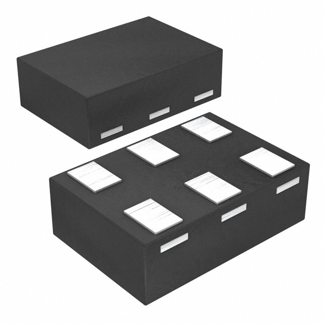
TPS62733DRYT
ActiveSTEP DOWN CONVERTER WITH BYPASS MODE FOR ULTRA LOW POWER WIRELESS APPLICATIONS
Deep-Dive with AI
Search across all available documentation for this part.

TPS62733DRYT
ActiveSTEP DOWN CONVERTER WITH BYPASS MODE FOR ULTRA LOW POWER WIRELESS APPLICATIONS
Technical Specifications
Parameters and characteristics for this part
| Specification | TPS62733DRYT |
|---|---|
| Applications | Converter, Bluetooth (BLT) |
| Mounting Type | Surface Mount |
| Number of Outputs | 1 |
| Operating Temperature [Max] | 85 °C |
| Operating Temperature [Min] | -40 C |
| Package / Case | 6-UFDFN |
| Supplier Device Package | 6-SON (1.45x1) |
| Voltage - Input [Max] | 3.9 V |
| Voltage - Input [Min] | 1.9 V |
| Voltage - Output | 2.3 V |
Pricing
Prices provided here are for design reference only. For realtime values and availability, please visit the distributors directly
| Distributor | Package | Quantity | $ | |
|---|---|---|---|---|
| Digikey | Cut Tape (CT) | 1 | $ 1.52 | |
| 10 | $ 1.37 | |||
| 25 | $ 1.29 | |||
| 100 | $ 1.10 | |||
| Digi-Reel® | 1 | $ 1.52 | ||
| 10 | $ 1.37 | |||
| 25 | $ 1.29 | |||
| 100 | $ 1.10 | |||
| N/A | 698 | $ 1.64 | ||
| 1027 | $ 1.64 | |||
| Tape & Reel (TR) | 250 | $ 1.03 | ||
| 500 | $ 0.90 | |||
| 750 | $ 0.75 | |||
| 1250 | $ 0.75 | |||
| 1750 | $ 0.72 | |||
| 2500 | $ 0.70 | |||
| 6250 | $ 0.67 | |||
| 12500 | $ 0.65 | |||
| Texas Instruments | SMALL T&R | 1 | $ 1.26 | |
| 100 | $ 0.97 | |||
| 250 | $ 0.71 | |||
| 1000 | $ 0.51 | |||
Description
General part information
TPS62733 Series
The TPS62730 is a high frequency synchronous step-down DC-DC converter optimized for ultra low-power wireless applications. The device is optimized to supply TI’s Low-Power Wireless sub 1-GHz and 2.4-GHz RF transceivers and System-On-Chip (SoC) solutions. The TPS62730 reduces the current consumption drawn from the battery during TX and RX mode by a high efficient step-down voltage conversion. The device provides an output current of up to 100 mA and allows the use of tiny and low-cost chip inductors and capacitors. With an input voltage range of 1.9 V to 3.9 V, the device supports Li-primary battery chemistries such as Li-SOCl2, Li-SO2, Li-MnO2, and also two cell alkaline batteries.
The TPS62730 features an Ultra Low-Power bypass mode with typical 30-nA current consumption to support sleep and low power modes of TI’s CC2540BluetoothLow Energy and CC430 SoC solutions. In this bypass mode, the output capacitor of the DC-DC converter is connected through an integrated typical 2.1-Ω bypass switch to the battery.
In DC-DC operation mode the device provides a fixed output voltage to the system. With a switch frequency up to 3 MHz, the TPS62730 features low output ripple voltage and low noise even with a small 2.2-µF output capacitor. The automatic transition into bypass mode during DC-DC operation prevents an increase of output ripple voltage and noise once the DC-DC converter operates close to 100% duty cycle. The device automatically enters bypass mode once the battery voltage falls below the transition threshold VIT BYP. The TPS62730 is available in a 1 × 1.5-mm26-pin USON package.
Documents
Technical documentation and resources


