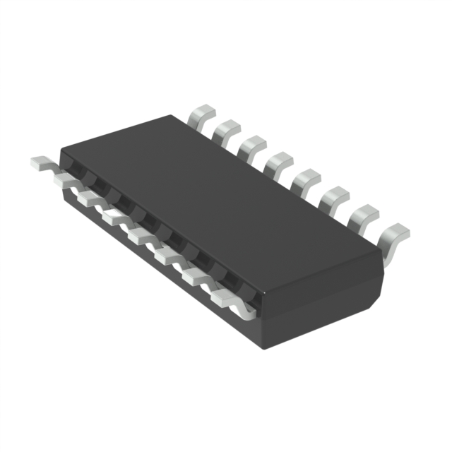
MC74VHCT257ADG
ObsoleteQUAD 2-CHANNEL MULTIPLEXER (MUX) WITH 3-STATE OUTPUTS
Deep-Dive with AI
Search across all available documentation for this part.

MC74VHCT257ADG
ObsoleteQUAD 2-CHANNEL MULTIPLEXER (MUX) WITH 3-STATE OUTPUTS
Deep-Dive with AI
Technical Specifications
Parameters and characteristics for this part
| Specification | MC74VHCT257ADG |
|---|---|
| Circuit [custom] | 4 |
| Circuit [custom] | 2:1 |
| Current - Output High, Low [custom] | 8 mA |
| Current - Output High, Low [custom] | 8 mA |
| Independent Circuits | 1 |
| Mounting Type | Surface Mount |
| Operating Temperature [Max] | 125 °C |
| Operating Temperature [Min] | -55 °C |
| Package / Case | 16-SOIC |
| Package / Case [x] | 0.154 in |
| Package / Case [y] | 3.9 mm |
| Supplier Device Package | 16-SOIC |
| Type | Multiplexer |
| Voltage - Supply [Max] | 5.5 V |
| Voltage - Supply [Min] | 4.5 V |
| Voltage Supply Source | Single Supply |
Pricing
Prices provided here are for design reference only. For realtime values and availability, please visit the distributors directly
| Distributor | Package | Quantity | $ | |
|---|---|---|---|---|
Description
General part information
MC74VHCT257A Series
The MC74VHCT257A is an advanced high speed CMOS quad 2-channel multiplexer fabricated with silicon gate CMOS technology. It achieves high speed operation similar to equivalent Bipolar Schottky TTL while maintaining CMOS low power dissipation.It consists of four 2-input digital multiplexers with common select (S) and enable (OE)bar inputs. When (OE)bar is held High, selection of data is inhibited and all the outputs go Low.The select decoding determines whether the A or B inputs get routed to the corresponding Y outputs.The VHCT inputs are compatible with TTL levels. This device can be used as a level converter for interfacing 3.3 V to 5.0 V because it has full 5 V CMOS level output swings.The VHCT257A input structures provide protection when voltages between 0 V and 5.5 V are applied, regardless of the supply voltage. The output structures also provide protection when VCC= 0 V. These input and output structures help prevent device destruction caused by supply voltage input/output voltage mismatch, battery backup, hot insertion, etc.The internal circuit is composed of three stages, including a buffer output which provides high noise immunity and stable output. The inputs tolerate voltages up to 7 V, allowing the interface of 5 V systems to 3 V systems.
Documents
Technical documentation and resources


